SCI7654M

Features: An input voltage can be boosted double/triple/quadruple to negative potential. Input voltages: 2.4 to 5.5V (quadruple boosting), 2.4 to 7.3V (triple boosting), 2.4 to 11.0V (double boosting) Excellent vol tage conversion efficiency: 95% (Typ.) Large output current: 20 mA (Max.) during q...

product image

SCI7654M Picture
SeekIC No. : 004486016 Detail

SCI7654M: Features: An input voltage can be boosted double/triple/quadruple to negative potential. Input voltages: 2.4 to 5.5V (quadruple boosting), 2.4 to 7.3V (triple boosting), 2.4 to 11.0V (double boosti...

floor Price/Ceiling Price

Part Number:
SCI7654M
Supply Ability:
5000

Price Break

  • Qty
  • 1~5000
  • Unit Price
  • Negotiable
  • Processing time
  • 15 Days
Total Cost: $ 0.00

SeekIC Buyer Protection PLUS - newly updated for 2013!

  • Escrow Protection.
  • Guaranteed refunds.
  • Secure payments.
  • Learn more >>

Month Sales

268 Transactions

Rating

evaluate  (4.8 stars)

Upload time: 2024/4/25

Payment Methods

All payment methods are secure and covered by SeekIC Buyer Protection PLUS.

Notice: When you place an order, your payment is made to SeekIC and not to your seller. SeekIC only pays the seller after confirming you have received your order. We will also never share your payment details with your seller.
Product Details

Description


Features:

An input voltage can be boosted double/triple/quadruple to negative potential.
Input voltages: 2.4 to 5.5V (quadruple boosting), 2.4 to 7.3V (triple boosting), 2.4 to 11.0V (double boosting)
Excellent vol tage conversion efficiency: 95% (Typ.)
Large output current: 20 mA (Max.) during quadruple boosting
Built-in voltage regulator (for stable voltage output)
Built-in reference voltage source for accurate regulation: 1.5 ±0.05V (CT0)
Regulator output voltage temperature gradient function: 0.04, 0.15, 0.35, 0.55%/°C
Low current consumption: 130 A (Typ.)
Low standby current: 5.0 A (Max.)
Built-in oscillator circuit
5/6-time voltage boosting in negative potential by serial connection
Package: SCI7654M0A SSOP2-16pin (plastic), SCI7654C0A DIP-16pin (plastic)


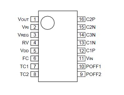
Pinout

  Connection Diagram


Specifications

Rating
Symbol
Min.
Max.
Unit
Remark
Input Power Voltage
VIN
-26.0/N
VDD +0.3
V
N=Boosting time; at VIN pin
Input Pin Voltage
VI
VIN -0.3
VDD +0.3
V
POFF1, POFF2 TC1, TC2, FC pins
Output Pin Voltage 1
V0C1
VIN -0.3
VDD +0.3
V
At C1P and C2P pins
Output Pin Voltage 2
V0C2
2 *VIN -0.3
VIN +0.3
V
At C1N pin
Output Pin Voltage 3
V0C3
3 *VIN -0.3
2 *VIN +0.3
V
At C2N pin
Output Pin Voltage 4
V0C4
4 *VIN -0.3
3 *VIN +0.3
V
At C3N pin
Regulator Input Power Voltage
VRI
N* VIN -0.3
VDD +0.3
V
N=Boosting time; at VRI pin
Regulator Input Pin Voltage
VRV
N* VIN -0.3
VDD +0.3
V
N=Boosting time; at RV pin
Output Voltage
V0
N *VIN -0.3
VDD +0.3
V
N=Boosting time; at VOUT and VREG pins
Input Current
IIN
-
80
mA
At VIN pin
Output Current
IOUT
-
N4: 20
N>4: 80/N
mA
N=Boosting time; at VOUTand VREG pins
Allowable Loss
Pd
-
210
mW
-
Operating Temperature
Topr
-30
85
°C
-
Storage Temperature
Tstg
-55
150
°C
-
Soldering Temperature and Time
Tsol
-
260•10
°C.S
Temperature at leads


Description

The SCI7654M is a highly efficient, but low power-consumption DC-to-DC converter based on the advanced CMOS technologies. SCI7654M can generate an output voltage double/triple/quadruple times higher than the input (in negative direction) if 4/3/2 external capacitors are attached.

With a built-in voltage regulator, the SCI7654M can provide a stable output by setting the DC/DC output to any voltage via two external resistors. This is optimum to the LCD panel power supply as the stable output can have the negative temperature gradient required for an LCD panel.


Customers Who Bought This Item Also Bought

Margin,quality,low-cost products with low minimum orders. Secure your online payments with SeekIC Buyer Protection.
Inductors, Coils, Chokes
Sensors, Transducers
Isolators
Computers, Office - Components, Accessories
View more