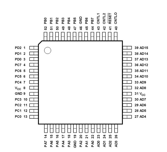
Features: FLASH IN-SYSTEM PROGRAMMABLE (ISP)
PERIPHERAL FOR 8-BIT MCUS
DUAL BANK FLASH MEMORIES
UP TO 2 Mbit OF PRIMARY FLASH
MEMORY (8 Uniform Sectors, 32K x8)
UP TO 256 Kbit SECONDARY FLASH
MEMORY (4 Uniform Sectors)
Concurrent operation: READ from one
memory while erasing and writing the other
UP TO 256 Kbit BATTERY-BACKED SRAM
27 RECONFIGURABLE I/O PORTS
ENHANCED JTAG SERIAL PORT
PLD WITH MACROCELLS
Over 3000 Gates of PLD: CPLD and DPLD
CPLD with 16 Output Macrocells (OMCs)
and 24 Input Macrocells (IMCs)
DPLD - user defined internal chip select decoding
27 INDIVIDUALLY CONFIGURABLE I/O
PORT PINS
The can be used for the following functions:
MCU I/Os
PLD I/Os
Latched MCU address output
Special function I/Os.
16 of the I/O ports may be configured as
open-drain outputs.
IN-SYSTEM PROGRAMMING (ISP) WITH JTAG
Built-in JTAG compliant serial port allows
full-chip In-System Programmability
Efficient manufacturing allow easy
product testing and programming
Use low cost FlashLINK cable with PC
PAGE REGISTER
Internal page register that can be used to
expand the microcontroller address space
by a factor of 256
PROGRAMMABLE POWER MANAGEMENT
HIGH ENDURANCE:
100,000 Erase/WRITE Cycles of Flash Memory
1,000 Erase/WRITE Cycles of PLD
15 Year Data Retention
5V±10% SINGLE SUPPLY VOLTAGE
STANDBY CURRENT AS LOW AS 50APinout Specifications
|
Symbol |
Parameter |
Min. |
Max. |
Unit |
|
TSTG
|
Storage Temperature |
65
|
125
|
°C |
|
TLEAD |
Lead Temperature during Soldering (20 seconds max.)1 |
|
235 |
°C |
|
VIO |
Input and Output Voltage (Q = VOH or Hi-Z) |
0.6 |
7.0 |
V |
|
VCC |
Supply Voltage |
0.6 |
7.0 |
V |
|
VPP |
Device Programmer Supply Voltage |
0.6 |
14.0 |
V |
|
VESD |
Electrostatic Discharge Voltage (Human Body model)2 |
2000 |
2000 |
V |
DescriptionThe PSD8XXFX family of memory systems for mi- rocontrollers (MCUs) brings In-System-Program-mability (ISP) to Flash memory and programmable logic. The result is a simple and flexible solution for embedded designs. PSD devices combine many of the peripheral functions found in MCU based applications.
Table 1 summarizes all the devices in the PSD834F2, PSD853F2, PSD854F2. The CPLD in the PSD devices features an opti- mized macrocell logic architecture. The PSD mac- rocell was created to address the unique requirements of embedded system designs. PSD834F2, PSD853F2, PSD854F2 allow direct connection between the system ad-dress/data bus, and the internal PSD registers, to simplify communication between the MCU and other supporting devices.
The PSD device includes a JTAG Serial Program-ming interface, to allow In-System Programming (ISP) of the entire device. PSD834F2, PSD853F2, PSD854F2 feature reduces de- velopment time, simplifies the manufacturing flow,and dramatically lowers the cost of field upgrades.Using ST's special Fast-JTAG programming, a design can be rapidly programmed into the PSD in as little as seven seconds.
The innovative PSD8XXFX family solves key problems faced by designers when managing dis-crete Flash memory devices, such as: First-time In-System Programming (ISP) Complex address decoding Simultaneous read and write to the device.
The JTAG Serial Interface block of PSD834F2, PSD853F2, PSD854F2 allows In-System Programming (ISP), and eliminates the need for an external Boot EPROM, or an external program- mer. To simplify Flash memory updates, program execution is performed from a secondary Flash memory while the primary Flash memory is being updated. This solution of PSD834F2, PSD853F2, PSD854F2 avoids the complicated hardware and software overhead necessary to im-plement IAP.
ST makes available a software development tool,PSDsoft Express, that generates ANSI-C compli-ant code for use with your target MCU. This code of PSD834F2, PSD853F2, PSD854F2 allows you to manipulate the non-volatile memory (NVM) within the PSD. Code examples of PSD834F2, PSD853F2, PSD854F2 are also provided for: Flash memory IAP via the UART of the host MCU Memory paging to execute code across several PSD memory pages Loading, reading, and manipulation of PSD macrocells by the MCU.

 SD834F2 Data Sheet


