Features: Word-organized reprogrammable nonvolatile memory in n-channel floating-gate technology (E2PROM)
128X8-bit organization
Supply voltage 5 V
Serial 2-line bus for data input and output (I2C Bus)
Reprogramming mode, 10 ms erase/write cycle
Reprogramming by means of on-chip control (without external control)
Check for end of programming process
Data retention > 10 years
More than 104 reprogramming cycles per address
Compatible with SDA 2516. Exception:Conditions for total erase and current consumption ICC.
Pinout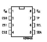 Specifications
| Parameter |
Symbol |
Limit Values |
Unit |
| min. |
max. |
| Supply voltage |
VCC |
0.3 |
6 |
V |
| Input voltage |
VI |
0.3 |
6 |
V |
| Power dissipation |
PD |
|
130 |
mW |
| Storage temperature |
Tstg |
40 |
125 |
°C |
| Thermal resistance (system-air) |
R th SA |
|
100 |
K/W |
| Junction temperature |
Tj |
|
85 |
°C |
DescriptionI2C Bus Interface
The I2C Bus SDA2516-5 is a bidirectional 2-line bus for the transfer of data between various integrated circuits. SDA2516-5 consists of a serial data line SDA and a serial clock line SCL. The data line of SDA2516-5 requires an external pull-up resistor to VCC (open drain output stage).
The possible operational states of the I2C Bus SDA2516-5 are shown in figure 1. In the quiescent state, both lines SDA and SCL are high, i.e. the output stage of the data line of SDA2516-5 is disabled. As long a SCL remains "1", information changes on the data bus SDA2516-5 indicate the start or the end of data transfer between two components.
The transition on SDA from "1" to "0" is a start condition, the transition from "0" to "1" a stop condition. During a data transfer the information on the data bus will only change while the clock line SCL is "0". The information on SDA is valid as long as SCL is "1".
In conjunction with an I2C Bus SDA2516-5 system, the memory component can operate as a receiver and as a transmitter (slave receiver or slave transmitter). Between a start and stop condition, information about SDA2516-5 is always transmitted in byte-organized form. Between the trailing edge of the eighth clock pulse and a ninth acknowledge clock pulse, the memory component sets the SDA line to low as a confirmation of reception, if the chip select conditions have been met. During the output of data, the data output of the memory is high in impedance during the ninth clock pulse (acknowledge master).
The signal timing required for the operation of the I2C Bus is summarized in figure 2.
Control Functions of the I2C Bus
The memory component of SDA2516-5 is controlled by the controller (master) via the I2C Bus in two operating modes: read-out cycle, and reprogramming cycle, including erase and write to a memory address. In both operating modes, the controller, as transmitter, has to provide 3 bytes and an additional acknowledge clock pulse to the bus after the start condition. During a memory read, at least nine additional clock pulses are required to accept the data of SDA2516-5 from the memory and the acknowledge master, before the stop condition may follow. In the case of programming, the active programming process is only started by the stop condition after data input (see figure 3).
The SDA2516-5 select word contains the 3 chip select bits CS0, CS1 and CS2, thus allowing 8 memory chips to be connected in parallel. Chip select is achieved when the three control bits logically correspond to the selected conditions at the select inputs.
Check for End of Programming or Abortion of Programming Process
If the SDA2516-5 is addressed during active reprogramming by entering CS/E, the programming process is terminated. If, however, it is addressed by entering CS/A, the entry will be ignored. Only after programming has been terminated will the chip respond to CS/A. SDA2516-5 allows the user to check whether the end of the programming process has been reached (see figure 3).
Memory Read
After the input of the first two control words CS/E and WA, the resetting of the start condition and the input of a third control word CS/A, the memory is set ready to read. During acknowledge clock nine, the memory information about SDA2516-5 is transferred in parallel mode to the shift register. Subsequent to the trailing edge of the acknowledge clock, the data output is low impedance and the first data bit can be sampled, (see figure 4).
With every shift clock, an additional bit reaches the output. After reading a byte, the internal address counter SDA2516-5 is automatically incremented when the master receiver switches the data line to "low" during the ninth clock (acknowledge master). Any number of memory locations can thus be read one after the other. At address 128, an overflow to address 0 is not initiated. With the stop condition, the data output returns to high-impedance mode. The internal sequence control of the memory component of SDA2516-5 is reset from the read to the quiescent with the stop condition.
Memory Reprogramming
The reprogramming cycle of a memory word comprises an erase and a subsequent write process. During erase, all eight bits of the selected word are set into "1" state. During write, "0" states are generated according to the information in the internal data register, i.e. according to the third input control word.
After the 27th and the last clock of the control word input, the active programming process is started by the stop condition. The active reprogramming process is executed under onchip control.
The SDA2516-5 required for reprogramming depends on component deviation and data patterns. Therefore, with rated supply voltage, the erase/write process extends over max. 20 ms, or more typically, 10 ms. In the case of data word input without write request (write request is defined as data bit in data register set to "0"), the write process is suppressed and the programming time is shortened. During a subsequent programming of an already erased memory address, the erase process of SDA2516-5 is suppressed again, so that the reprogramming time is also shortened.
Important: Switch-On Mode and Chip Reset
After the supply voltage VDD has been connected, the data output of SDA2516-5 will be in the high-impedance mode. As a rule, the first operating mode to be entered, should be the read process of a word address. As a result of the built-in "power-on reset" circuit, programming requests will not be accepted immediately after the supply voltage of SDA2516-5 has been switched on.
Total Erase
Enter the control word CS/E, load the address register SDA2516-5 with address 0 and the data register with FF (hex) to erase the entire contents of the memory. Switch input CS2 to "open" immediately prior to generating the stop condition. The subsequent stop condition triggers a total erase. Upon termination of "total erase", CS2 must be reconnected to either 0 V or ³ 4.5 V.

 SDA2516-5 Data Sheet