Features: • Wide frequency output by PLL technology.• Quick delivery of samples and short lead mass production time.• Excellent environmental capability.• Output enable function (OE) and stand-by function (ST) can be used for current consumption applications.• Pin com...
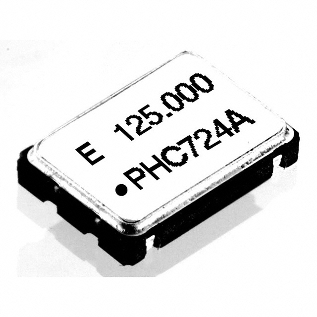
SG-8002DB: Features: • Wide frequency output by PLL technology.• Quick delivery of samples and short lead mass production time.• Excellent environmental capability.• Output enable funct...
SeekIC Buyer Protection PLUS - newly updated for 2013!
268 Transactions
All payment methods are secure and covered by SeekIC Buyer Protection PLUS.
Item |
Symbol |
PT/ST |
PH/SH |
PC/SC |
Remarks | |
Specifications | ||||||
Output frequency range |
f0 |
1.0000 MHz to 125.0000 MHz |
||||
Power source voltage |
Max. supply voltage |
V DD-GND |
-0.5 V to +7.0 V |
|||
Operating voltage |
VDD |
5.0 V±0.5 V 3.3 ± 0.3 V |
3.0 V ±0.3 V: f0 66.7 MHz(PC/SC) | |||
Temperature range |
Storage temperature |
TSTG |
-55 °C to +125 °C |
|||
Operating temperature |
TOPR |
-20 °C to +70 °C (-40 °C to +85 °C) |
40 °C to +85 °C |
Refer to page 4."Frequency range" | ||
Soldering condition |
TSOL |
Twice at under +260 °C within 10 s or under +230 °C within 3 min. |
||||
Frequency stability |
∆f/f0 |
B: ±50 x 10-6 C: ± 100 x 10-6 M: ±100 x 10-6 |
B,C: -20 °C to +70 °C, M:-40 °C to 85 °C | |||
Current consumption |
Iop |
45 mA Max. |
28 mA Max. |
No load condition, Max. frequency range | ||
Output disable current |
IOE |
30 mA Max. |
16 mA Max. |
OE=GND(PT,PH,PC) | ||
Standby current |
IST |
50 µA Max. |
ST=GND(ST,SH,SC) | |||
Duty |
tw/ t |
- |
40 % to 60 % |
C-MOS load: 1/2VDD level | ||
40 % to 60 % |
- |
TTL load: 1.4 V level | ||||
High output voltage |
VOH |
VDD -0.4 V Min. |
IOH=-16 mA(PT/ST,PH/SH),-8 mA(PC/SC) | |||
Low output voltage |
VOL |
0.4 V Max. |
IOL= 16 mA(PT/ST,PH/SH), 8 mA(PC/SC) | |||
Output load condition (fan out) |
TTL |
N |
5 TTL Max. |
- |
||
C-MOS |
CL |
15 pF Max. |
||||
Output enable/disable input voltage |
VIH |
2.0 V Min. |
0.7 x VDD Min. |
Max. frequency and Max. operating voltage range | ||
VIL |
0.8 V Max. |
0.2 x VDD Max. |
ST , OE terminal | |||
Output rise time |
C-MOS level |
tTLH |
- |
4 ns Max. |
4 ns Max. |
|
TTL level |
4 ns Max. |
- |
- |
|||
Output fall time |
C-MOS level |
tTHL |
4 ns Max. |
- |
- |
|
TTL level | - | - | 4 ns Max. | |||
Oscillation start up time |
tOSC |
10 ms Max. |
Time at minimum operating voltage to be 0 s | |||
Aging |
tOSC |
±5 x 10⁻⁶ / year Max. |
Ta = +25 ˚C, VDD = 5.0 V / 3.3 V, First year | |||
Shock resistance |
S.R. |
±20 x 10-6 Max. |
Three drops on a hard board from 750 mm or excitation test with 29400 m/s2 x 0.3 ms x 1/2sine wave in 3 directions |