Features: • Original Hitachi architecture
• 32-bit internal architecture
• General register machine
Sixteen 32-bit general registers
Six 32-bit control registers (including 3 added for DSP use)
Four 32-bit system registers
• RISC (Reduced Instruction Set Computer) type instruction set
Fixed 16-bit instruction length for improved code efficiency
Load-store architecture (basic operations are executed between registers)
Delayed branch instructions reduce pipeline disruption during branches
C-oriented instruction set
• Instruction execution time: One instruction per cycle (16.7 ns/instruction at 60 MHz operation)
• Address space: Architecture supports 4 Gbytes
• On-chip multiplier: Multiply operations (32 bits * 32 bits 64 bits) and multiply-and-accumulate operations (32 bits * 32 bits + 64 bits 64 bits) executed in two to four cycles
• Five-stage pipeline
• DSP engine
Multiplier
Arithmetic logic unit (ALU)
Shifter
DSP registers
• Multiplier
16 bits * 16 bits 32 bits
Single-cycle multiplier
• DSP registers
Two 40-bit data registers
Six 32-bit data registers
Modulo register (MOD, 32 bits) added to control registers
Repeat counter (RC) added to status register (SR)
Repeat start register (RS, 32 bits) and repeat end register (RE, 32 bits)
added to control registers
• DSP data bus
Extended Harvard architecture
Simultaneous access to two data buses and one instruction bus
• Parallel processing
Maximum of four parallel processes
ALU operations, multiplication, and two loads or stores
• Address processors
Two address processors
Address operations to access two memories
• DSP data addressing modes
Increment and index
Each with or without modulo addressing
• Repeat control: Zero-overhead repeat (loop) control
• Instruction set
16-bit length (in case of load or store only)
32-bit length (including ALU operations and multiplication)
Added SuperH microcontroller instructions for accessing DSP registers
• Fifth and last pipeline stage is DSP stage
• Mixed instruction/data type cache
• Maximum of 4 kbytes
• 4-way set-associative type
• 16-byte line length
• 64 cache tag entries
• 16-byte write-back buffer
• Selection of write-through or write-back mode for data writes
• LRU replacement algorithm
• Can also be used as 2-kbyte cache and 2-kbyte RAM (2-way cache mode)
• Mixed instruction/data cache, instruction cache, or data cache mode can be set
• 1-cycle reads, 2-cycle writes (in write-back mode)
• 16 priority levels can be set
• On-chip supporting module interrupt vector numbers can be set
• 41 internal interrupt sources
• The E-DMAC interrupt (EINT) is input to the INTC as the OR of 21 EtherC and E-DMAC interrupt sources (max.). Thus, from the viewpoint of the INTC, there is one EtherC/E-DMAC interrupt source.
• Five external interrupt pins (NMI, IRL0 to IRL3)
15 external interrupt sources (encoded input) can also be selected for pins IRL0 to IRL3 (IRL interrupts)
• IRL interrupt vector number setting can also be selected (selection of auto vector or external vector)
• Provision for IRQ interrupt setting (low-level, rising-edge, falling-edge,both-edge detection)
• Interrupt generation based on independent or sequential conditions for channels A, B, C, D
Three sequential setting patterns: A B C D, B C D,C D
• Settable break conditions: Address, data (channels C and D only), bus master (CPU/DMAC), bus cycle (instruction fetch/data access), read/write,operand cycle (byte/word/longword)
• User break interrupt generated on occurrence of break condition
• Processing can be stopped before or after instruction execution in instruction fetch cycle
• Break with specification of number of executions (channels C and D only) Settable number of executions: max. 212 1 (4095)
• PC trace function
Branch source/branch destination can be traced in branch instruction fetch(max. 8 addresses (4 pairs))
• Address space divided into five areas (CS0 to CS4, max. linear 32 Mbytes each)
Memory types such as DRAM, synchronous DRAM, burst ROM, can be specified for each area
Two synchronous DRAM spaces (CS2, CS3); CS3 also supports DRAM
Bus width (8, 16, 32 bits) can be selected for each area
Wait state insertion control for each area
Control signal output for each area
Endian can be set for CS2 and CS4
• Cache
Cache area/cache-through area selection by access address
Selection of write-through or write-back mode
• Refresh functions
CAS-before-RAS refreshing (auto refreshing) or self-refreshing
Refresh interval settable by means of refresh counter and clock select setting
Concentrated refreshing according to refresh count setting (1, 2, 4, 6, 8)
Refresh request output possible (REFOUT)
• Direct DRAM interface
Multiplexed row address/column address output
Fast page mode burst transfer and continuous access when reading
EDO mode
TP cycle generation to secure RAS precharge time
• Direct synchronous DRAM interface
Multiplexed row address/column address output
Bank-active mode (valid for CS3 only)
Selection of burst read/single write mode or burst read/burst write mode
• Bus arbitration (BRLS, BGR)
• Refresh counter can be used as interval timer
Interrupt request generated on compare match (CMI interrupt request signal)
• 4-Gbyte address space, maximum 16M (16,777,216) transfers
• Selection of 8-bit, 16-bit, 32-bit, or 16-byte transfer data length
• Parallel execution of CPU instruction processing and DMA operation possible in case of cache hit
• Selection of dual address or single address mode
Single address (data transfer rate of one transfer unit in one bus cycle)
Dual address (data transfer rate of one transfer unit in two bus cycles)
When synchronous DRAM is connected, 16-byte continuous read continuous write transfer is possible (dual)
When synchronous DRAM is connected, one-clock single address transfer is possible up to 30 MHz
• Cycle stealing or burst transfer
• Relative channel priorities can be set (fixed mode/round robin mode)
• DMA transfer is possible for the following devices:
External memory, on-chip memory, on-chip supporting modules (excluding DMAC, BSC, UBC, cache)
• External requests, DMA transfer requests from on-chip supporting modules, auto requests
• Interrupt request (DEIn) can be issued to CPU at end of data transfer
• DACK used for DREQ sampling (however, there is always one overrun as there is one acceptance before first DACK)
• 4-kbyte X-RAM
• 4-kbyte Y-RAM
• Transfer possible between EtherC and external memory/on-chip memory
• 16-byte burst transfer possible
• Single address transfer
• Chain block transfer
• 32-bit transfer data width
• 4-Gbyte address space
• MAC (Media Access Control) functions
Data frame assembly/disassembly (IEEE802.3-compliant frames)
CSMA/CD link management (collision avoidance, processing in case of collision)
CRC processing
Built-in FIFOs (512 bytes each for transmission and reception)
Supports full-duplex transmission/reception
Transmitting and receiving short and long packets
• Compatible with MII (Media Independent Interface) standard
Converts 8-bit stream data from MAC level to MII nibble stream (4 bits)
Station management (STA) functions
18 TTL-level signals
Variable transfer rate: 10/100 Mbps
• Magic Packet™* (with WOL (Wake On LAN) output)
• Asynchronous mode
Data length: 7 or 8 bits
Stop bit length: 1 or 2
Parity: Even, odd, or none
Receive error detection: Parity errors, framing errors, overrun errors
Break detection
• Synchronous mode
One serial communication format (8-bit data length)
Receive error detection: Overrun errors
• IrDA mode (conforming to IrDA 1.0)
• Simultaneous transmission/reception (full-duplex) capability
Half-duplex communication used for IrDA communication
• Built-in dedicated baud rate generator allows selection of bit rate
• Built-in 16-stage transmit and receive FIFOs enable high-speed,continuous communication
• Internal or external (SCK) transmit/receive clock source
• Four interrupt sources
Transmit FIFO data empty
Break
Receive FIFO data full
Receive error
• Built-in modem control functions (RTS, CTS)
• Detection of transmit and receive FIFO register data quantity and number of receive FIFO register transmit data errors
• Timeout error (DR) can be detected during reception
Pinout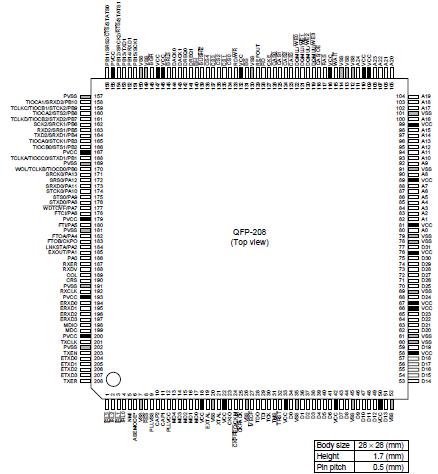 Specifications
|
Item |
Symbol |
Ratings |
Units |
| Power supply voltage |
VCC |
0.3 to 7.0 |
V |
| Input voltage |
Vin |
0.3 to PVCC + 0.3 |
V |
| Operating temperature |
Topr |
20 to 75 |
°C |
| Storage temperature |
Tstg |
55 to 125 |
°C |
Note: Permanent damage to the chip may result if the maximum ratings are exceeded.

 SH7615 Data Sheet


