Mounting Style
: SMD/SMT
Packaging
: Tray
Package / Case
: CBGA-63
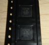
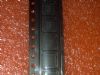
DescriptionThe SI5321-G-BC is one member of the SI5321 series.The Si5321 is a precision clock multiplier that exceeds the requirements of high-speed communication systems, including OC-192/OC-48 and 10 Gigabit Ethernet. This device phase locks to an input clock in the 19, 39, 78, 155, 311 or 622 MHz frequency range and generates a frequency-multiplied clock output that can be configured for operation in the 19, 39, 78, 155, 622, 1244, or 2488 MHz frequency range. Silicon Laboratories DSPLL(TM) technology provides PLL functionality with unparalleled performance.
Features of the SI5321-G-BC are:(1)ultra-low jitter clock output with jitter generation as low as 0.3 PSrms; (2)no external components (other than a resistor and bypassing); (3)input clock ranges at 19, 39, 78, 155,311, or 622 MHz; (4)output clock ranges at 19, 39, 78, 155,; (5)311, 622, 1244, or 2488 MHz ; (6)maximum range includes 693 MHz for 10 GbE FEC support; (7)selectable loop bandwidth; (8)loss-of-signal alarm output; (9)low power; (10)small size (9x9 mm); (11)backwards compatible with Si5320.
The absolute maximum ratings of the SI5321-G-BC can be summarized as:(1)3.3 V DC supply voltage:-0.5 to 3.6V;(2)LVTTL input voltage:-0.3 to Vdd33+0.3V;(3)maximum current any output PIN:±50 mA;(4)storage temperature:-55 to 150;(5)operating junction temperature:-55 to 150.Permanent device damage may occur if the Absolute Maximum Ratings are exceeded. Functional operation should be restricted to the conditions as specified in the operational sections of this data sheet. Exposure to absolute maximum rating conditions for extended periods may affect device reliability.Jitter transfer is defined as the ratio of output signal jitter to input signal jitter for a specified jitter frequency. The jitter transfer characteristic determines the amount of input clock jitter that passes to the outputs. The DSPLL technology used in the Si5321 provides tightly-controlled jitter transfer curves because the PLL gain parameters are determined by digital circuits that do not vary over supply voltage, process, and temperature. In a system application of the SI5321-G-BC, a well-controlled transfer curve minimizes the output clock jitter variation from board to board and provides more consistent system level jitter performance.
Parameters: | Technical/Catalog Information | SI5321-G-BC |
| Vendor | Silicon Laboratories Inc |
| Category | Integrated Circuits (ICs) |
| Type | Clock Multiplier |
| Voltage - Supply | 3.135 V ~ 3.465 V |
| Number of Outputs | 1 |
| Input | LVTTL |
| Output | CML |
| Frequency-Max | 2.4GHz |
| Package / Case | 63-CBGA |
| Packaging | Tray |
| Operating Temperature | -20°C ~ 85°C |
| Drawing Number | * |
| Lead Free Status | Lead Free |
| RoHS Status | RoHS Compliant |
| Other Names | SI5321 G BC
SI5321GBC
336 1274 ND
3361274ND
336-1274
|

 SI5321-G-BC Data Sheet