Features: ` Highest Performance Fixed-Point Digital Signal Processor (DSP) SM320C6201
6.67-ns Instruction Cycle Time
150-MHz Clock Rate
Eight 32-Bit Instructions/Cycle
1200 MIPS
` Highest Performance Fixed-Point Digital Signal Processor (DSP) SMJ320C6201B
6.67-ns Instruction Cycle Time
150-MHz Clock Rate
Eight 32-Bit Instructions/Cycle
1200 MIPS
` VelociT™E Advanced Very Long Instruction Word (VLIW) 'C6200 CPU Core
Eight Independent Functional Units:
Six ALUs (32-/40-Bit)
Two 16-Bit Multipliers (32-Bit Results)
Load-Store Architecture With 32 32-Bit General-Purpose Registers
Instruction Packing Reduces Code Size
All Instructions Conditional
` Instruction Set Features
Byte-Addressable (8-, 16-, 32-Bit Data)
32-Bit Address Range
8-Bit Overflow Protection
Saturation
Bit-Field Extract, Set, Clear
Bit-Counting
Normalization
` 1M-Bit On-Chip SRAM
512K-Bit Internal Program/Cache (16K 32-Bit Instructions)
512K-Bit Dual-Access Internal Data (64K Bytes) Organized as a Single Block ('6201)
512K-Bit Dual-Access Internal Data (64K Bytes) Organized as Two Blocks for Improved Concurrency ('6201B)
` 32-Bit External Memory Interface (EMIF)
Glueless Interface to Synchronous Memories: SDRAM and SBSRAM
Glueless Interface to Asynchronous Memories: SRAM and EPROM
` Four-Channel Bootloading Direct-Memory-Access (DMA) Controller with an Auxiliary Channel
` 16-Bit Host-Port Interface (HPI)
Access to Entire Memory Map
` Two Multichannel Buffered Serial Ports (McBSPs)
Direct Interface to T1/E1, MVIP, SCSA Framers
ST-Bus-Switching Compatible
Up to 256 Channels Each
AC97-Compatible
Serial Peripheral Interface (SPI) Compatible (MotorolaE)
` Two 32-Bit General-Purpose Timers
` Flexible Phase-Locked Loop (PLL) Clock Generator
` IEEE-1149.1 (JTAG†) Boundary-Scan Compatible
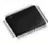
` 429-Pin BGA Package (GLE Suffix) ('6201)
` 429-Pin BGA Package (GLP Suffix) ('6201B)
` CMOS Technology
0.25-mm/5-Level Metal Process ('6201)
0.18-mm/5-Level Metal Process ('6201B)
` 3.3-V I/Os, 2.5-V Internal ('6201)
` 3.3-V I/Os, 1.8-V Internal ('6201B)SpecificationsSupply voltage range, CVDD (see Note 1) for 'C6201 . . . . . . . . . . . . . . . . . . . . . . . . . . . . . .. . . . . 0.3 V to 3 V
Supply voltage range, CVDD (see Note 1) for 'C6201B . . . . . . . . . . . . . . . . . . . . . . . . . . . . . . . . 0.3 V to 2.3 V
Supply voltage range, DVDD (see Note 1) . . . . . . . . . . . . . . . . . . . . . . . . . . . . . . . . . . . . . . . . . . .. . 0.3 V to 4 V
Input voltage range . . . . . . . . . . . . . . . . . . . . . . . . . . . . . . . . . . . . . . . . . . . . . . . . . . . . . . . . . . . . . 0.3 V to 4 V
Output voltage range . . . . . . . . . . . . . . . . . . . . . . . . . . . . . . . . . . . . . . . . . . . . . . . . . . . . . . . . . . . . 0.3 V to 4 V
Operating case temperature range, TC (S temperature) ..............................................................55C to 105
(M temperature) .................................................................55 to 125
Storage temperature range, Tstg ....................................................................................................55 to 150
† Stresses beyond those listed under "absolute maximum ratings" may cause permanent damage to the device. These are stress ratings only, and functional operation of the device at these or any other conditions beyond those indicated under "recommended operating conditions" is not implied. Exposure to absolute-maximum-rated conditions for extended periods may affect device reliability.
NOTE 1: All voltage values are with respect to VSS.DescriptionThe SM320C6201 CPU fetches VelociTI advanced very-long instruction words (VLIW) (256 bits wide) to supply up to eight 32-bit instructions to the eight functional units during every clock cycle. The VelociTI VLIW architecture features controls by which all eight units do not have to be supplied with instructions if they are not ready to execute. The first bit of every 32-bit instruction determines if the next instruction belongs to the same execute packet as the previous instruction, or whether it should be executed in the following clock as a part of the next execute packet. Fetch packets are always 256 bits wide; however, the execute packets can vary in size. The variable-length execute packets are a key memory-saving feature, distinguishing the 'C6200† CPU from other VLIW architectures.
The SM320C6201 CPU features two sets of functional units. Each set contains four units and a register file. One set contains functional units .L1, .S1, .M1, and .D1; the other set contains units .D2, .M2, .S2, and .L2. The two register files each contain 16 32-bit registers for a total of 32 general-purpose registers. The two sets of functional units, along with two register files, compose sides A and B of the CPU (see Figure 3 and Figure 4). The four functional units on each side of the CPU can freely share the 16 registers belonging to that side. Additionally, each side features a single data bus connected to all the registers on the other side, by which the two sets of functional units can access data from the register files on the opposite side. While register access by functional units on the same side of the CPU as the register file can service all the units in a single clock cycle, register access using the register file across the CPU supports one read and one write per cycle.
Another key feature of the 'C6200 CPU is the load/store architecture, where all instructions operate on registers (as opposed to data in memory). Two sets of data-addressing units (.D1 and .D2) are responsible for all data transfers between the register files and the memory. The data address driven by the .D units allows data addresses generated from one register file to be used to load or store data to or from the other register file. The 'C6200 CPU supports a variety of indirect addressing modes using either linear- or circular-addressing modes with 5- or 15-bit offsets. All instructions are conditional, and most can access any one of the 32 registers. Some registers, however, are singled out to support specific addressing or to hold the condition for conditional instructions (if the condition is not automatically "true"). The two .M functional units are dedicated for multiplies. The two .S and .L functional units perform a general set of arithmetic, logical, and branch functions with results vailable every clock cycle.
The SM320C6201 processing flow begins when a 256-bit-wide instruction fetch packet is fetched from a program memory.
The 32-bit instructions destined for the individual functional units are "linked" together by "1" bits in the least significant bit (LSB) position of the instructions. The instructions that are "chained" together for simultaneous execution (up to eight in total) compose an execute packet. A "0" in the LSB of an instruction breaks the chain, effectively placing the instructions that follow it in the next execute packet. If an execute packet crosses the fetch packet boundary (256 bits wide), the assembler places it in the next fetch packet, while the remainder of the current fetch packet is padded with NOP instructions. The number of execute packets within a fetch packet can vary from one to eight. Execute packets are dispatched to their respective functional units at the rate of one per clock cycle and the next 256-bit fetch packet is not fetched until all the execute packets from the current fetch packet have been dispatched. After decoding, the instructions simultaneously drive all active functional units for a maximum execution rate of eight instructions every clock cycle. While most results are stored in 32-bit registers, they can be subsequently moved to memory as bytes or half-words as well. All load and store instructions are byte-, half-word, or word-addressable.

 SM320C6201 Data Sheet