Features: · Reduces Systemic EMI.
· Modulates external source clock.
· 3 - 5 Volt power supply.
· 14 to 120 MHz.operating frequency range.
· Output is multiplied or divided by 1, 2 or 4.
· Digitally controlled modulation.
· TTL/CMOS compatible outputs.
· Fout modulation centered around reference.
· Compliant with all major CISC, RISC and DSP processors.
· Low short term jitter.
· Synchronous output enable.
· Power down mode for low current operation.
· Available in 16 pin SOIC package.Application` Desktop/Laptop Computer
` Modems
` Scanners, Printers, Copiers, Fax Machines, MFP's
` Disk and CD-ROM Drives
` Automotive and EmbeddedSystems
` Networking, LAN/WAN
` Digital Cameras, Games
` LCD displaysPinout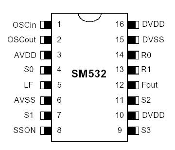 Specifications
This device contains circuitry to protect the inputs against damage due to high static voltages or electric fields; however, precautions should be taken to avoid application of any voltage higher than the absolute maximum rated voltages to this circuit. For proper operation, Vin and Vout should be constrained to the range, VSS < ( Vin or Vout) < VDD. All digital inputs are tied high or low internally. Refers to electrical specifications for operating supply range.
| Item |
Symbol |
Min. |
Max. |
Units |
| Supply Voltage |
VDD |
0 |
6.0 |
VDC |
| Input, relative to VSS |
VIRvss |
-0.3 |
VDD +0.3 |
VDC |
| Output, relative to VSS |
VORvss |
-0.3 |
VDD +0.3 |
VDC |
| AVDD relative to DVDD |
DVpp |
-100 |
+100 |
mv |
| AVSS relative to DVSS |
DVss |
-100 |
+100 |
mv |
| Temperature, Operating |
TOP |
0 |
+ 70 |
|
| Temperature, Storage |
TST |
- 65 |
+ 150 |
|
DescriptionThe IMI SM532 is a Spectrum Spread Clock Modulator designed for the purpose of reducing the Electro- Magnetic Interference (EMI) found in today's high speed digital systems. The SM532 is well suited for a wide range of digital system applications that require a reduction of radiated energy. This unwanted radiated energy is usually found in the odd harmonics of digital system clocks. By modulating the frequency of the digital clock, measured EMI at the fundamental and harmonic frequencies is greatly reduced. This reduction in radiated energy can significantly reduce the cost of complying with regulatory requirements and time to market, without degrading clock and timing signals.
The IMI SM532 is extremely versatile and flexible in that program control is available for each of the operating modes. Program control is provided for Input Frequency, Output Frequency Multiplication, Output Bandwidth, Modulation ON/OFF and Fout state during Power Down Mode. Depending on the range of operation, the output clock, Fout, can be a multiple (1, 2, 4) or a division (1, 1/2, 1/4) of the input frequency. The power-down mode adds the flexibility of operating in a completely static mode for reduced standby current and simplified system board testing.
There are many benefits to using the SM532 Low EMI Clock Modulator. The most important benefit is reducing the amount of clock related EMI by as much as 12 - 18 dB, depending on the application. SM532 is available with only Center-Spread frequency modulation. Refer to SM530 for Down-Spread frequency modulation and other functions.

 SM532 Data Sheet


