Features: LVTTL Receiver and Eight Line Drivers Configured as an 8-Port M-LVDS Repeater − SN65MLVD1282 LVTTL Receivers and Eight Line Drivers Configured as Dual 4-Port M-LVDS Repeaters − SN65MLVD129Drivers Meet or Exceed the M-LVDS Standard (TIA/EIA-899)Low-Voltage Differential 30-T...
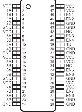
SM65MLVD129DGGR: Features: LVTTL Receiver and Eight Line Drivers Configured as an 8-Port M-LVDS Repeater − SN65MLVD1282 LVTTL Receivers and Eight Line Drivers Configured as Dual 4-Port M-LVDS Repeaters −...
SeekIC Buyer Protection PLUS - newly updated for 2013!
268 Transactions
All payment methods are secure and covered by SeekIC Buyer Protection PLUS.
Features: IEEE1284 parallel port terminator filter and integrated protection devicesEMI noise elim...
Features: LVTTL Receiver and Eight Line Drivers Configured as an 8-Port M-LVDS Repeater − SN...
LVTTL Receiver and Eight Line Drivers Configured as an 8-Port M-LVDS Repeater − SN65MLVD128
2 LVTTL Receivers and Eight Line Drivers Configured as Dual 4-Port M-LVDS Repeaters − SN65MLVD129
Drivers Meet or Exceed the M-LVDS Standard (TIA/EIA-899)
Low-Voltage Differential 30-Ω to 55-Ω Line Drivers for Data Rates(1) Up to 250 Mbps or Clock Frequencies Up to 125 MHz
Power Up/Down Glitch Free
Controlled Driver Output Voltage Transition Times for Improved Signal Quality
Bus Pins High Impedance When Disabled or VCC 1.5 V
Output-to-Ouput Skew tsk(o) 160 ps Part-to-Part Skew tsk(pp) 800 ps
Single 3.3-V Voltage Supply
Bus Pin ESD Protection Exceeds 9 kV
Packaged in 48-Pin TSSOP (DGG)

|
SN65MLVD128, 129 | |||
| Supply voltage range(2), VCC |
−0.5 V to 4 V | ||
| Input voltage range, VI | D, EN |
−0.5 V to 4 V | |
| Output voltage range, VO | A or B |
−1.8 V to 4 V | |
| Electrostatic discharge | Human Body Model(3) | A, B |
±9 kV |
| All pins |
±4 kV | ||
| Charged-Device Model(4) | All pins |
±1500 V | |
| Machine Model(5) | All pins |
200 V | |
| Continuous power dissipation |
See Dissipation Rating Table | ||
The SN65MLVD128 and SN65MLVD129 are LVTTL-to-M−LVDS translators/repeaters. Outputs comply with the M−LVDS standard (TIA/EIA-899) and are optimized for data rates up to 250 Mbps, and clock frequencies up to 125 MHz. The driver outputs have been designed to support multipoint buses presenting loads as low as 30 Ω and incorporates controlled transition times for backbone operation.
M-LVDS compliant devices allow for 32 nodes on a common bus, providing a high-speed replacement for RS-485 devices when lower common-mode voltage range and lower output signaling levels are acceptable. The SN65MLVD128 and SN65MLVD129 provide separate driver enables, allowing for independent control of each output signal.
Intended applications for these devices include transmission of clock signals from a central clock module, as well as translation and buffering of data or control signals for transmission through a controlled impedance backplane or cable.