Features: Processed to MIL-PRF-38535 (QML)
Advanced Multibus Architecture With Three Separate
16-Bit Data Memory Buses and One Program Memory Bus
40-Bit Arithmetic Logic Unit (ALU) Including a 40-Bit Barrel
Shifter and Two Independent 40-Bit Accumulators
17 x 17-Bit Parallel Multiplier Coupled to a 40-Bit Dedicated Adder for
Non-Pipelined Single-Cycle Multiply/Accumulate (MAC) Operation
Compare, Select, and Store Unit (CSSU) for the Add/Compare Selection of the Viterbi Operator
Exponent Encoder to Compute an Exponent Value of a 40-Bit Accumulator Value in a Single Cycle
Two Address Generators With Eight Auxiliary Registers and
Two Auxiliary Register Arithmetic Units (ARAUs)
Data Bus With a Bus Holder Feature
Extended Addressing Mode for 8M x 16-Bit Maximum Addressable External Program Space
128K x 16-Bit On-Chip RAM Composed of:
Eight Blocks of 8K x 16-Bit On-Chip Dual-Access Program/Data RAM
Eight Blocks of 8K x 16-Bit On-Chip Single-Access Program RAM
16K x 16-Bit On-Chip ROM Configured for Program Memory
Enhanced External Parallel Interface (XIO2)
Single-Instruction-Repeat and Block-Repeat Operations for Program Code
Block-Memory-Move Instructions for Better Program and Data Management
Instructions With a 32-Bit Long Word Operand
Instructions With Two- or Three-Operand Reads
Arithmetic Instructions With Parallel Store and Parallel Load
Conditional Store Instructions
Fast Return From Interrupt
On-Chip Peripherals
Software-Programmable Wait-State Generator and Programmable Bank-Switching
On-Chip Programmable Phase-Locked Loop (PLL) Clock Generator With External Clock Source
One 16-Bit Timer
Six-Channel Direct Memory Access(DMA) Controller
Three Multichannel Buffered Serial Ports(McBSPs)
8/16-Bit Enhanced Parallel Host-Port Interface (HPI8/16)
Power Consumption Control With IDLE1, IDLE2, and IDLE3 Instructions With Power-Down Modes
CLKOUT Off Control to Disable CLKOUT
On-Chip Scan-Based Emulation Logic, IEEE Std 1149.1† (JTAG) Boundary Scan Logic
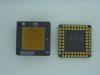
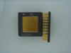
164-Pin Ceramic Quad Flatpack (CQFP) (HFG Suffix)
10-ns Single-Cycle Fixed-Point Instruction Execution Time (100 MIPS)
3.3-V I/O Supply Voltage
1.5-V Core Supply Voltage
55°C to 115°C Operating Temperature Range, QML Processing
Pinout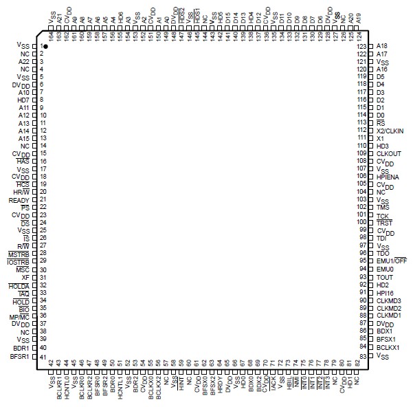 Specifications
Supply voltage I/O range, DVDD . . . . . . . . . . . . . . . . . . . . . . . . . . . . . . . . . . . . . . . . . . . 0.3 V to 4.0 V
Supply voltage core range, CVDD . . . . . . . . . . . . . . . . . . . . . . . . . . . . . . . . . . . . . . . . . . 0.3 V to 2.0 V
Input voltage range . . . . . . . . . . . . . . . . . . . . . . . . . . . . . . . . . . . . . . . . . . . . . . . . . . . . 0.3 V to 4.5 V
Output voltage range . . . . . . . . . . . . . . . . . . . . . . . . . . . . . . .. . . . . . . . . . . . . . . . . . . . 0.3 V to 4.5 V
Thermal resistance, Junction-to-Case, JC . . . . . . . . . . . . . . . . . . .... . . . . . . . . . . . . . . . . . . 1.82°C/W
Operating case temperature range, TC . . . . . . . . . . . . . . . . . . . . ..... . . . . . . . . . . . . . 55°C to 115°C
Storage temperature range, Tstg . . . . . . . . . . . . . . . . . . . . . . . . . . . . . . . . . . . . . . . . 55°C to 150°C
DescriptionThe SMJ320VC5416 fixed-point, digital signal processor (DSP) (hereafter referred to as the 5416 unless otherwise specified) is based on an advanced modified Harvard architecture that has one program memory bus and three data memory buses. This processor provides an arithmetic logic unit (ALU) with a high degree of parallelism, application-specific hardware logic, on-chip memory, and additional on-chip peripherals. The basis of the operational flexibility and speed of this DSP is a highly specialized instruction set.
Separate program and data spaces allow simultaneous access to program instructions and data, providing a high degree of parallelism. Two read operations and one write operation can be performed in a single cycle. Instructions with parallel store and application-specific instructions can fully utilize this architecture. In addition, data can be transferred between data and program spaces. Such parallelism supports a powerful set of arithmetic, logic, and bit-manipulation operations that can all be performed in a single machine cycle. The SMJ320VC5416 also includes the control mechanisms to manage interrupts, repeated operations, and function calls.

 SMJ320VC5416 Data Sheet