SN10KHT5573

Features: • 10KH Compatible• ECL and TTL Control Inputs• Noninverting Outputs• Flow-Through Architecture Optimizes PCB Layout• Center Pin VCC, VEE, and GND Configurations Minimize High-Speed Switching Noise• Package Options Include Small Outline Packages and S...

product image

SN10KHT5573 Picture
SeekIC No. : 004496059 Detail

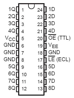
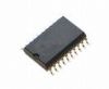
SN10KHT5573: Features: • 10KH Compatible• ECL and TTL Control Inputs• Noninverting Outputs• Flow-Through Architecture Optimizes PCB Layout• Center Pin VCC, VEE, and GND Configuratio...

floor Price/Ceiling Price

Part Number:
SN10KHT5573
Supply Ability:
5000

Price Break

  • Qty
  • 1~5000
  • Unit Price
  • Negotiable
  • Processing time
  • 15 Days
Total Cost: $ 0.00

SeekIC Buyer Protection PLUS - newly updated for 2013!

  • Escrow Protection.
  • Guaranteed refunds.
  • Secure payments.
  • Learn more >>

Month Sales

268 Transactions

Rating

evaluate  (4.8 stars)

Upload time: 2025/12/24

Payment Methods

All payment methods are secure and covered by SeekIC Buyer Protection PLUS.

Notice: When you place an order, your payment is made to SeekIC and not to your seller. SeekIC only pays the seller after confirming you have received your order. We will also never share your payment details with your seller.
Product Details

Description


Features:

• 10KH Compatible
• ECL and TTL Control Inputs
• Noninverting Outputs
• Flow-Through Architecture Optimizes PCB Layout
• Center Pin VCC, VEE, and GND
  Configurations Minimize High-Speed
  Switching Noise
• Package Options Include "Small Outline"
  Packages and Standard Plastic 300-mil DIPs


Pinout

  Connection Diagram 


Specifications

Supply voltage range, VCC . . . . . . . . . . . . . . . . . . . . . . . . . . . . . . . . . . . . . . . . . . . . . . . . . . . . . . 0.5 V to 7 V
Supply voltage range, VEE . . . . . . . . . . . . . . . . . . . . . . . . . . . . . . . . . . . . . . . . . . . . . . . . . . . . . . . . 8 V to 0 V
Input voltage range, TTL (see Note 1) . . . . . . . . . . . . . . . . . . . . . . . . . . . . . . . . . . . . . . . . . . . . . .1.2 V to 7 V
Input voltage range, ECL . . . . . . . . . . . . . . . . . . . . . . . . . . . . . . . . . . . . . . . . . . . . . . . . . . . . . . . . .  VEE to 0 V
Input current range, TTL . . . . . . . . . . . . . . . . . . . . . . . . . . . . . . . . . . . . . . . . . . . . . . . . . . . . . . 30 mA to 5 mA
Current into any output in the low state . . . . . . . . . . . . . . . . . . . . . . . . . . . . . . . . . . . . . . . . . . . . . . . . . .96 mA
Voltage applied to any output in the disabled or power-off state . . . . . . . . . . . . . . . . . . . . . . . . 0.5 V to 5.5 V
Voltage applied to any output in the high state . . . . . . . . . . . . . . . . . . . . . . . . . . . . . . . . . . . . . . .0.5 V to VCC
Operating free-air temperature range . . . . . . . . . . . . . . . . . . . . . . . . . . . . . . . . . . . . . . . . . . . . . . . .0°C to 75°C
Storage temperature range . . . . . . . . . . . . . . . . . . . . . . . . . . . . . . . . . . . . . . . . . . . . . . . . . . . . .65°C to 150°C
† Stresses beyond those listed under "absolute maximum ratings" may cause permanent damage to the device. These are stress ratings only and
functional operation of the device at these or any other conditions beyond those indicated under "recommended operating conditions" is not
implied. Exposure to absolute-maximum-rated conditions for extended periods may affect device reliability.
NOTE 1: The TTL input voltage ratings may be exceeded provided the input current ratings are observed.


Description

This octal ECL-to-TTL translator is designed to provide efficient translation between a 10KH ECL signal environment and a TTL signal environment. SN10KHT5573  is designed specifically to improve the performance and density of ECL-to-TTL CPU/bus-oriented functions such as memory address drivers, clock drivers, and bus-oriented receivers and transmitters.

The eight latches of the SN10KHT5573 are transparent D-type latches. While latch enable (LE) is low, the Q outputs follow the data (D) inputs. When LE is high, the Q outputs are latched at the levels that were set up at the D inputs.

A buffered output-enable (OE) input can be used to place the eight outputs in either a normal logic state (high or low logic levels) or a high-impedance state. In the high-impedance state, the outputs neither load nor drive the bus lines significantly. The high-impedance third state and increased drive provide the capability to drive bus lines without need for interface or pullup components. Output-enable OE does not affect the internal operations of the latches. Old data can be retained or new data can be entered while the outputs are off.The SN10KHT5573 is characterized for operation from 0° to 75°C.


Customers Who Bought This Item Also Bought

Margin,quality,low-cost products with low minimum orders. Secure your online payments with SeekIC Buyer Protection.
Potentiometers, Variable Resistors
Sensors, Transducers
Memory Cards, Modules
Motors, Solenoids, Driver Boards/Modules
Resistors
View more