Features: ` Members of the Texas Instruments WidebusTM Family
` State-of-the-Art EPIC-IIBTM BiCMOS Design Significantly Reduces Power Dissipation
` ESD Protection Exceeds 2000 V Per MIL-STD-883, Method 3015; Exceeds 200 V Using Machine Model (C = 200 pF, R = 0)
` Typical VOLP (Output Ground Bounce) < 1 V at VCC = 5 V, TA = 25°C
` Distributed VCC and GND Pin Configuration Minimizes High-Speed Switching Noise
` Flow-Through Architecture Optimizes PCB Layout
` High-Drive Outputs (32-mA IOH, 64-mA IOL)
` Package Options Include Plastic Thin Shrink Small-Outline (DGG), 300-mil Shrink Small-Outline (DL) Packages and 380-mil Fine-Pitch Ceramic Flat (WD) Package Using 25-mil Center-to-Center Spacings
Pinout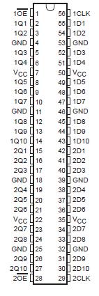 Specifications
Supply voltage range, VCC . . . . . . . . . . . . . . . . . . . . . . . . . . . . . . . . . . . . . . . . . . . . . . . 0.5 V to 7 V
Input voltage range, VI (see Note 1) . . . . . . . . . . . . . . . . . . . . . . . . . . . . . . . . . . . . . . . . 0.5 V to 7 V
Voltage range applied to any output in the high or power-off state, VO . . . . . . . . .. . . 0.5 V to 5.5 V
Current into any output in the low state, IO: SN54ABT16821 . . . . . . . . . . . . . . . . . . . . . . . . . . .96 mA
SN74ABT16821 . . . . . . . . . . . . . . . . . . . . . .. . . . .128 mA
Input clamp current, IIK (VI < 0) . . . . . . . . . . . . . . . . . . . . . . . . . . . . . . . . . . . . . . . . . . . . . . . ..18 mA
Output clamp current, IOK (VO < 0) . . . . . . . . . . . . . . . . . . . . . . . . . . . . . . . . . . . . . . . .. . . . . . .50 mA
Package thermal impedance, JA (see Note 2): DGG package . . . . . . . . . . . . . . . . . . . . . . . . . 81°C/W
DL package . . . . . . . . . . . . . . . . . . . . . . . . . . . 74°C/W
Storage temperature range, Tstg . . . . . . . . . . . . . . . . . . . . . . . . . . . . . . . . . . . . . . . . 65°C to 150°C
† Stresses beyond those listed under "absolute maximum ratings" may cause permanent damage to the device. These are stress ratings only, and functional operation of the device at these or any other conditions beyond those indicated under "recommended operating conditions" is not implied. Exposure to absolute-maximum-rated conditions for extended periods may affect device reliability.
NOTES: 1. The input and output negative-voltage ratings may be exceeded if the input and output clamp-current ratings are observed.
2. The package thermal impedance is calculated in accordance with EIA/JEDEC Std JESD51.
DescriptionThese 20-bit flip-flops feature 3-state outputs of SN54ABT16821 designed specifically for driving highly capacitive or relatively low-impedance loads. SN54ABT16821 is particularly suitable for implementing wider buffer registers, I/O ports, bidirectional bus drivers with parity, and working registers.
The SN54ABT16821 can be used as two 10-bit flip-flops or one 20-bit flip-flop. The 20 flip-flops are edge-triggered D-type flip-flops. On the positive transition of the clock (CLK) input, the device provides true data at the Q outputs.
A buffered output-enable (OE) input of SN54ABT16821 can be used to place the ten outputs in either a normal logic state (high or low logic level) or a high-impedance state. In the high-impedance state, the outputs of SN54ABT16821 neither load nor drive the bus lines significantly. The high-impedance state and increased drive provide the capability to drive bus lines without need for interface or pullup components.
OE does not affect the internal operation of the flip-flops. Old data of SN54ABT16821 can be retained or new data can be entered while the outputs are in the high-impedance state.
To ensure the high-impedance state during power up or power down, OE should be tied to VCC through a pullup resistor; the minimum value of the resistor SN54ABT16821 is determined by the current-sinking capability of the driver.
The SN54ABT16821 is characterized for operation over the full military temperature range of 55°C to 125°C. The SN74ABT16821 is characterized for operation from 40°C to 85°C.

 SN54ABT16821 Data Sheet


