Features: ` Members of the Texas Instruments WidebusTM Family
` State-of-the-Art EPIC-IIBTM BiCMOS Design Significantly Reduces Power Dissipation
` Latch-Up Performance Exceeds 500 mA Per JEDEC Standard JESD-17
` Typical VOLP (Output Ground Bounce) < 1 V at VCC = 5 V, TA = 25°C
` High-Impedance State During Power Up and Power Down
` Distributed VCC and GND Pin Configuration Minimizes High-Speed Switching Noise
` Flow-Through Architecture Optimizes PCB Layout
` High-Drive Outputs (32-mA IOH, 64-mA IOL)
` Package Options Include Plastic 300-mil Shrink Small-Outline (DL) Package and 380-mil Fine-Pitch Ceramic Flat (WD)Package Using 25-mil Center-to-Center Spacings
Pinout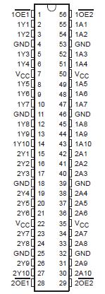 Specifications
Supply voltage range, VCC . . . . . . . . . . . . . . . . . . . . . . . . . . . . . . . . . . . . . . . . . . . . . . . . 0.5 V to 7 V
Input voltage range, VI (see Note 1) . . . . . . . . . . . . . . . . . . . . . . . . . . . . . . . . . . . . . . . . 0.5 V to 7 V
Voltage range applied to any output in the high or power-off state, VO . . . . . . . . . . . . 0.5 V to 5.5 V
Current into any output in the low state, IO: SN54ABT16827 . . . . . . . . . . . . . . .. . . . . . . . . . . . . 96 mA
SN74ABT16827 . . . . . . . . . . . . . . . . . . . . . . . . . .. 128 mA
Input clamp current, IIK (VI < 0) . . . . . . . . . . . . . . . . . . . . . . . . . . . . . . . . . . . . . . . . . . . . . . . .. 18 mA
Output clamp current, IOK (VO < 0) . . . . . . . . . . . . . . . . . . . . . . . . . . . . . . . . . . . . . . . .. . . . . . . 50 mA
Package thermal impedance, JA (see Note 2): DL package . . . . . . . . . . . . . . . . . . . . . . . . . . . 74°C/W
Storage temperature range, Tstg . . . . . . . . . . . . . . . . . . . . . . . . . . . . . . . . . . . . . . . . 65°C to 150°C
† Stresses beyond those listed under "absolute maximum ratings" may cause permanent damage to the device. These are stress ratings only, and functional operation of the device at these or any other conditions beyond those indicated under "recommended operating conditions" is not implied. Exposure to absolute-maximum-rated conditions for extended periods may affect device reliability.
NOTES: 1. The input and output negative-voltage ratings may be exceeded if the input and output clamp-current ratings are observed.
2. The package thermal impedance is calculated in accordance with EIA/JEDEC Std JESD51.
DescriptionThe SN54ABT16827 are noninverting 20-bit buffers composed of two 10-bit sections with separate output-enable signals. For either 10-bit buffer section, the two output-enable (1OE1 and 1OE2 or 2OE1 and 2OE2) inputs of SN54ABT16827 must both be low for the corresponding Y outputs to be active. If either output-enable input is high, the outputs of that 10-bit buffer section are in the high-impedance state.
When VCC is between 0 and 2.1 V, the SN54ABT16827 is in the high-impedance state during power up or power down. However, to ensure the high-impedance state above 2.1 V, OE should be tied to VCC through a pullup resistor; the minimum value of the resistor SN54ABT16827 is determined by the current-sinking capability of the driver.
The SN54ABT16827 is characterized for operation over the full military temperature range of 55°C to 125°C. The SN74ABT16827 is characterized for operation from 40°C to 85°C.

 SN54ABT16827 Data Sheet


