Features: ` Output Ports Have Equivalent 25- Series Resistors, So No External Resistors Are Required
` State-of-the-Art EPIC-IIBTM BiCMOS Design Significantly Reduces Power Dissipation
` Flow-Through Architecture Optimizes PCB Layout
` Latch-Up Performance Exceeds 500 mA Per JEDEC Standard JESD-17
` Typical VOLP (Output Ground Bounce) < 1 V at VCC = 5 V, TA = 25°C
` Package Options Include Plastic Small-Outline (DW) Package, Ceramic Chip Carriers (FK), and Plastic (NT) and Ceramic (JT) DIPs
Pinout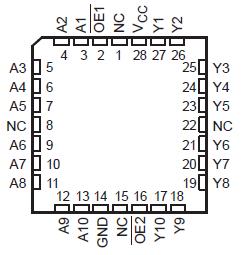
SpecificationsSupply voltage range, VCC . . . . . . . . . . . . . . . . . . . . . . . . . . . . . . . . . . . . . . . . . . .. 0.5 V to 7 V
Input voltage range, VI (see Note 1) . . . . . . . . . . . . . . . . . . . . . .. . . . . . . . . . . . . . 0.5 V to 7 V
Voltage range applied to any output in the high or power-off state, VO . . . . . . . 0.5 V to 5.5 V
Current into any output in the low state, IO: SN54ABT2827 . . . . . . . . . . . . . . . . . . . . . . . . 96 mA
SN74ABT2827 . . . . . . . . . . . . . . . . . . . . . . . 128 mA
Input clamp current, IIK (VI < 0) . . . . . . . . . . . . . . . . . . . . . . . . . . . . . . . . . . . . . . . . . . . .18 mA
Output clamp current, IOK (VO < 0) . . . . . . . . . . . . . . . . . . . . . . . . . . . . . . . . . . . . . . . . . . 50 mA
Package thermal impedance, JA (see Note 2): DW package . . . . . . . . . . . . . . . . . . . . . . 81°C/W
NT package . . . . . . . . . . . . . . . . . . . . . . . 67°C/W
Storage temperature range, Tstg . . . . . . . . . . . . . . . . . . . . . . . . . . . . . . . . . . . . 65°C to 150°C
‡ Stresses beyond those listed under "absolute maximum ratings" may cause permanent damage to the device. These are stress ratings only, and functional operation of the device at these or any other conditions beyond those indicated under "recommended operating conditions" is not implied. Exposure to absolute-maximum-rated conditions for extended periods may affect device reliability.
NOTES: 1. The input and output negative-voltage ratings may be exceeded if the input and output clamp-current ratings are observed.
2. The package thermal impedance is calculated in accordance with EIA/JEDEC Std JESD51, except for through-hole packages, which use a trace length of zero.
DescriptionThese SN54ABT2827 10-bit buffers or bus drivers provide a high-performance bus interface for wide data paths or buses carrying parity.
The 3-state control gate of SN54ABT2827 is a 2-input AND gate with active-low inputs so that if either output-enable (OE1 or OE2) input is high, all ten outputs are in the high-impedance state. The SN54ABT2827 provide true data at their outputs.
To ensure the high-impedance state during power up or power down, OE should be tied to VCC through a pullup resistor; the minimum value of the resistor is determined by the current-sinking capability of the driver.The outputs, which are designed to source or sink up to 12 mA, include equivalent 25- series resistors to reduce overshoot and undershoot.The SN54ABT2827 is characterized for operation over the full military temperature range of 55°C to 125°C. The SN74ABT2827 is characterized for operation from 40°C to 85°C.

 SN54ABT2827 Data Sheet


