Pinout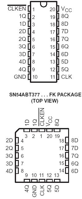 Specifications
Supply voltage range, V CC. . . . . . . . . . . . . . . . . . . . . . . . . . . . . . . . . . . . . . . . . . . . . . . . . . . . . . . . . . .. . . 0.5 V to 7 V
Input voltage range, VI (see Note 1) . . . . . . . . . . . . . . . . . . . . . .. . . . . . . . . . . . . . . . . . . . . . . . . . . .. . . . . 0.5 V to 7 V
Voltage range applied to any output in the high state or power-off state, VO . . . . . . . . . . . . .. . . . . . . . 0.5 V to 5.5 V
Current into any output in the low state, IO : SN54ABT377 . . . . . . . . . . . . . . . . . . . . . . . . . . . . . . . . . . . . . . . . . . 96 mA
SN74ABT377 . . . . . . . . . . . . . . ................... . . . . . . . . . . . . . . . . . . 128 mA
Input clamp current, I IK (VI< 0) . . . . . . . . . . . . . . . . . . . . . . . . . . . . . . . . . . . . . . . . . . . . . . . . . . . . . . .. . . . . . . 18 mA
Output clamp current, IOK (VO < 0) . . . . . . . . . . . . . . . . . . . . . . . . . . . . . . . . . . . . . . . . . . . . . . . . . . .. . ...... 50 mA
Maximum power dissipation at TA = 55o C (in still air) (see Note 2):DB package . . . . . . . . . . . . . . . . . . . . . . . . . . . 0.6 W
DW package . . . . . . . . . . . . . . . . . . . . . . . . . ....1.6 W
N package . . . . . . . . . . . . . . .. . . . . . . . . . ...... . 1.3 W
Storage temperature range . . . . . . . . . . . . . . . . . . . . . . . . . . . . . . . . . . . . . . . . . . . . . . . . . . . . . . . . . 65°C to 150°C
DescriptionThe SN54ABT377 are 8-bit positive-edge-triggered D-type flip-flops with a clock (CLK) input. SN54ABT377 is particularly suitable for implementing buffer and storage registers, shift registers, and pattern generators. Data (D) input information that meets the setup time requirements is transferred to the Q outputs on the positive-going edge of the clock pulse if the common clock-enable (CLKEN) input is low. Clock triggering occurs at a particular voltage level and is not directly related to the transition time of the positive-going pulse. When the buffered clock (CLK) input is at either the high or low level, the D input signal has no effect at the output. The circuits of SN54ABT377 are designed to prevent false clocking by transitions at CLKEN.
The SN74ABT377 is available in TI's shrink small-outline package (DB), which provides the same I/O pin count and functionality of standard small-outline packages in less than half the printed-circuit-board area. The SN54ABT377 is characterized for operation over the full military temperature range of 55°C to 125°C. The SN74ABT377 is characterized for operation from 40°C to 85°C.

 SN54ABT377 Data Sheet


