Features: State-of-the-Art EPIC-IIBTM BiCMOS Design Significantly Reduces Power Dissipation
Latch-Up Performance Exceeds 500 mA Per JEDEC Standard JESD-17
Typical VOLP (Output Ground Bounce) < 1 V at VCC = 5 V, TA = 25°C
High-Impedance State During Power Up and Power Down
High-Drive Outputs (32-mA IOH, 64-mA IOL)
Package Options Include Plastic Small-Outline (DW), Shrink Small-Outline (DB), and Thin Shrink Small-Outline (PW)
Packages, Ceramic Chip Carriers (FK), Ceramic Flat (W) Package, and Plastic (N) and Ceramic (J) DIPsPinout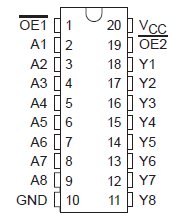 SpecificationsSupply voltage range, VCC . . . . . . . . . . . . . . . . . . . . . . . . . . . . . . . . . . . . . . . . . . . . . . . . . . . . . . . . . . 0.5 V to 7 V
Input voltage range, VI (see Note 1) . . . . . . . . . . . . . . . . . . . . . . . . . . . . . . . . . . . . . . . . . . . . . . . . . . 0.5 V to 7 V
Voltage range applied to any output in the high or power-off state, VO . . . . . . . . . . . . . . . . . . . 0.5 V to 5.5 V
Current into any output in the low state, IO: SN54ABT541 . . . . . . . . . . . . . . . . . . . . . . . . . . . . . . . . . . . . 96 mA
SN74ABT541B . . . . . . . . . . . . . . . . . . . . . . . . . . . . . . . . . . 128 mA
Input clamp current, IIK (VI < 0) . . . . . . . . . . . . . . . . . . . . . . . . . . . . . . . . . . . . . . . . . . . . . . . . . . . . . . . . . . . 18 mA
Output clamp current, IOK (VO < 0) . . . . . . . . . . . . . . . . . . . . . . . . . . . . . . . . . . . . . . . . . . . . . . . . . . . . . . . . 50 mA
Package thermal impedance, JA (see Note 2): DB package . . . . . . . . . . . . . . . . . . . . . . . . . . . . . . . . 115°C/W
DW package . . . . . . . . . . . . . . . . . . . . . . . . . . . . . . . . . 97°C/W
N package . . . . . . . . . . . . . . . . . . . . . . . . . . . . . . . . . . . 67°C/W
PW package . . . . . . . . . . . . . . . . . . . . . . . . . . . . . . . . 128°C/W
Storage temperature range, Tstg . . . . . . . . . . . . . . . . . . . . . . . . . . . . . . . . . . . . . . . . . . . . . . . . . . . 65°C to 150°C
‡ Stresses beyond those listed under "absolute maximum ratings" may cause permanent damage to the device. These are stress ratings only, and functional operation of the device at these or any other conditions beyond those indicated under "recommended operating conditions" is not implied. Exposure to absolute-maximum-rated conditions for extended periods may affect device reliability.
NOTES: 1. The input and output negative-voltage ratings may be exceeded if the input and output clamp-current ratings are observed.
2. The package thermal impedance is calculated in accordance with JESD 51, except for through-hole packages, which use a trace length of zero.DescriptionThe SN54ABT541 and SN74ABT541B octal buffers and line drivers are ideal for driving bus lines or buffering memory address registers. The SN54ABT541 and SN74ABT541B feature inputs and outputs on opposite sides of the package to facilitate printed circuit board layout.
The 3-state control gate is a two-input AND gate with active-low inputs so that if either output-enable (OE1 or OE2 ) input is high, all eight outputs are in the high-impedance state.
When VCC is between 0 and 2.1 V, the SN54ABT541 and SN74ABT541B are in the high-impedance state during power up or power down.However, to ensure the high-impedance state above 2.1 V, OE should be tied to V
CC through a pullup resistor;the minimum value of the resistor is determined by the current-sinking capability of the driver.
The SN54ABT541 is characterized for operation over the full military temperature range of 55°C to 125°C.
The SN74ABT541B is characterized for operation from 40°C to 85°C.

 SN54ABT541 Data Sheet


