Features: * Members of the Texas Instruments WidebusE Family
* B-Port Outputs Have Equivalent 25-W Series Resistors, So No External Resistors Are Required
* State-of-the-Art EPIC-IIBE BiCMOS Design Significantly Reduces Power Dissipation
* ESD Protection Exceeds 2000 V Per MIL-STD-883, Method 3015; Exceeds 200 V Using Machine Model (C = 200 pF, R = 0)
* Latch-Up Performance Exceeds 500 mA Per JEDEC Standard JESD-17
* Typical VOLP (Output Ground Bounce) < 1 V at VCC = 5 V, TA = 25°C
* High-Impedance State During Power Up nd Power Down
* Distributed VCC and GND Pin Configuration inimizes High-Speed Switching Noise
* Flow-Through Architecture Optimizes PCB ayout
* Bus Hold on Data Inputs Eliminates the eed for External Pullup/Pulldown esistors
* Package Options Include Plastic 300-mil hrink Small-Outline (DL) Package and380-mil Fine-Pitch Ceramic Flat (WD)Package Using 25-mil Center-to-Center Spacings
Pinout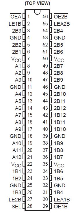 SpecificationsSupply voltage range, VCC . . . . . . . . . . . . . . . . . . . . . . . . . . . . . . . . . . . . . . . . . . . .. . 0.5 V to 7 V
Input voltage range, VI (see Note 1) . . . . . . . . . . . . . . . . . . . . . . . . . . . . . . . . . . . .. . 0.5 V to 7 V
Voltage range applied to any output in the high or power-off state, VO . . . . . . . . ...0.5 V to 5.5 V
Current into any output in the low state, IO: SN54ABTH162260 (A port) . . . . . . . . . ......... . 96 mA
SN74ABTH162260 (A port) . . . . . . . . . . . . . . . . . . . . . . ......................................................... 128 mA
B port . . . . . . . . . . . . . . . . . . . . . . . . . . . . . . . . . . . . . . . . . . ................................................... 30 mA
Input clamp current, IIK (VI < 0) . . . . . . . . . . . . . . . . . . . . . . . . . . . . . . . . . . . . . . . . . . . . . . 18 mA
Output clamp current, IOK (VO < 0) . . . . . . . . . . . . . . . . . . . . . . . . . . . . . . . . . . . . . . . . .. . .. 50 mA
Package thermal impedance, qJA (see Note 2): DL package . . . . . . . . . . . . . . . . . . . .. ...... . .74°C/W
Storage temperature range, Tstg . . . . . . . . . . . . . . . . . . . . . . . . . . . . . . . . . . . . .. . 65°C to 150°C DescriptionThe 'ABTH162260 are 12-bit to 24-bit multiplexed D-type latches used in applications where two separate data paths must be multiplexed onto, or demultiplexed from, a single data path. Typical applications include multiplexing and/or demultiplexing of address and data information in microprocessor or bus-interface applications. ABTH162260 is also useful in memory-interleaving applications.
Three 12-bit I/O ports (A1A12, 1B11B12, and 2B12B12) of ABTH162260 are available for address and/or data transfer. The output-enable (OE1B, OE2B, and OEA) inputs control the bus-transceiver functions. The OE1B and OE2B control signals also allow bank control in the A-to-B direction.
Address and/or data information of ABTH162260 can be stored using the internal storage latches. The latch-enable (LE1B, LE2B, LEA1B, and LEA2B) inputs are used to control data storage. When the latch-enable input is high, the latch is transparent. When the latch-enable input goes low, the data present at the inputs is latched and remains latched until the latch-enable input is returned high. The B-port outputs, ABTH162260 is designed to sink up to 12 mA, include equivalent 25-W series resistors to reduce overshoot and undershoot.

 SN54ABTH162260 Data Sheet


