SN54ABTH25245

Features: ` State-of-the-Art EPIC-II BE BiCMOS Design Significantly Reduces Power Dissipation` ESD Protection Exceeds 2000 V Per MIL-STD-883, Method 3015; Exceeds 200 V Using Machine Model (C = 200 pF, R = 0)` Latch-Up Performance Exceeds 500 mA Per JEDEC Standard JESD-17` Typical VOLP (Output Gro...

product image

SN54ABTH25245 Picture
SeekIC No. : 004496390 Detail

SN54ABTH25245: Features: ` State-of-the-Art EPIC-II BE BiCMOS Design Significantly Reduces Power Dissipation` ESD Protection Exceeds 2000 V Per MIL-STD-883, Method 3015; Exceeds 200 V Using Machine Model (C = 200 ...

floor Price/Ceiling Price

Part Number:
SN54ABTH25245
Supply Ability:
5000

Price Break

  • Qty
  • 1~5000
  • Unit Price
  • Negotiable
  • Processing time
  • 15 Days
Total Cost: $ 0.00

SeekIC Buyer Protection PLUS - newly updated for 2013!

  • Escrow Protection.
  • Guaranteed refunds.
  • Secure payments.
  • Learn more >>

Month Sales

268 Transactions

Rating

evaluate  (4.8 stars)

Upload time: 2025/12/24

Payment Methods

All payment methods are secure and covered by SeekIC Buyer Protection PLUS.

Notice: When you place an order, your payment is made to SeekIC and not to your seller. SeekIC only pays the seller after confirming you have received your order. We will also never share your payment details with your seller.
Product Details

Description


Features:

` State-of-the-Art EPIC-II BE BiCMOS Design Significantly Reduces Power Dissipation
` ESD Protection Exceeds 2000 V Per MIL-STD-883, Method 3015; Exceeds 200 V Using Machine Model (C = 200 pF, R = 0)
` Latch-Up Performance Exceeds 500 mA Per JEDEC Standard JESD-17
` Typical VOLP (Output Ground Bounce) < 1 V at VCC = 5 V, TA = 25°C
` High-Impedance State During Power Up and Power Down
` Designed to Facilitate Incident-Wave Switching for Line Impedances of 25 or Greater
` Distributed VCC and GND Pin Configuration Minimizes High-Speed Switching Noise
` Bus Hold on Data Inputs Eliminates the Need for External Pullup/Pulldown Resistors
` Package Options Include Plastic Small-Outline (DW) Package, Ceramic Chip Carriers (FK), and Standard Plastic (NT) and Ceramic (JT) DIPs


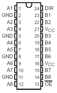
Pinout

  Connection Diagram


Specifications

Supply voltage range, VCC . . . . . . . . . . . . . . . . . . . . . . . . . . . . . . . . . . . . . . . .  . .0.5 V to 7 V
Input voltage range, VI (except I/O ports) (see Note 1) . . . . . . . . . . . . . . . . . . . .0.5 V to 7 V
Voltage range applied to any output in the disabled or power-off state, VO . . .0.5 V to 5.5 V
Voltage range applied to any output in the high state, VO . . . . . . . . . . . . . . . .  .0.5 V to VCC
Input clamp current, IIK (VI < 0) . . . . . . . . . . . . . . . . . . . . . . . . . . . . . . . . . .  . . .. . . . . 18 mA
Output clamp current, IOK (VO < 0) . . . . . . . . . . . . . . . . . . . . . . . . . . . . . . . . . . . . .  . . .50 mA
Current into any output in the low state, IO: SN74ABTH25245 (A port) . . . . .  . . . .. .. ..376 mA 
                                                                       SN74ABTH25245 (B port) . . . .  . . . . . . .. .128 mA
Package thermal impedance, JA (see Note 2): DW package . . . . . . . . . . . . . . . . . . . . 81°C/W
                                                                            NT package . . . . . . . . . . . . . . . . . . . . 67°C/W
Storage temperature range, Tstg . . . . . . . . . . . . . . . . . . . . . . . . . . . . . . . . .. .65°C to 150°C


Description

The 'ABTH25245 are 25- octal bus transceivers designed for asynchronous communication between data buses. SN54ABTH25245 improves both the performance and density of 3-state memory address drivers, clock drivers, and bus-oriented transceivers.

SN54ABTH25245 allows noninverted data transmission from the A bus to the B bus or from the B bus to the A bus, depending on the logic level at the direction-control (DIR) input. The output-enable (OE) input can disable the SN54ABTH25245 so that both buses are effectively isolated. When OE is low, the device is active.

These transceivers SN54ABTH25245 are capable of sinking 188 mA of IOL current, which facilitates switching 25- transmission lines on the incident wave. The distributed VCC and GND pins minimize switching noise for more-reliable system operation.

Active bus-hold circuitry of SN54ABTH25245 is provided to hold unused or floating data inputs at a valid logic level.

When VCC is between 0 and 2.1 V, the SN54ABTH25245 is in the high-impedance state during power up or power down. However, to ensure the high-impedance state above 2.1 V, OE should be tied to VCC through a pullup resistor; the minimum value of the resistor is determined by the current-sinking capability of the driver.

The SN54ABTH25245 is characterized for operation over the full military temperature range of 55°C to 125°C.

The SN74ABTH25245 is characterized for operation from 40°C to 85°C.


Customers Who Bought This Item Also Bought

Margin,quality,low-cost products with low minimum orders. Secure your online payments with SeekIC Buyer Protection.
Power Supplies - Board Mount
Resistors
Connectors, Interconnects
Batteries, Chargers, Holders
Test Equipment
Inductors, Coils, Chokes
View more