Features: ` Members of the Texas Instruments Widebus+™ Family
` State-of-the-Art EPIC-IIB™ BiCMOS Design Significantly Reduces Power Dissipation
` UBE ™ (Universal Bus Exchanger) Combines D-Type Latches and D-Type Flip-Flops for Operation in Transparent, Latched, or Clocked Mode
` Latch-Up Performance Exceeds 500 mA Per JEDEC Standard JESD-17
` Typical VOLP (Output Ground Bounce) < 0.8 V at VCC = 5 V, TA = 25°C
` High-Impedance State During Power Up and Power Down
` Distributed VCC and GND Pin Configuration Minimizes High-Speed Switching Noise
` High-Drive Outputs (32-mA IOH, 64-mA IOL)
` Bus Hold on Data Inputs Eliminates the Need for External Pullup/Pulldown Resistors
` Package Options Include 80-Pin Plastic Thin Quad Flat (PN) Package With 12 * 12-mm Body Using 0.5-mm Lead Pitch and 84-Pin Ceramic Quad Flat (HT) Package
Pinout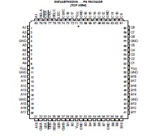 Specifications
Supply voltage range, VCC . . . . . . . . . . . . . . . . . . . . . . . . . . . . . . . . . . . . . . . . . . . . . . 0.5 V to 7 V
Input voltage range, VI (except I/O ports) (see Note 1) . . . . . . . . . . . . . . . . . . . . . . . 0.5 V to 7 V
Voltage range applied to any output in the high or power-off state, VO . . . . . . . . . . 0.5 V to 5.5 V
Current into any output in the low state, IO: SN54ABTH32318 . . . . . . . . . . . . . . . . .. . . . . . . . 96 mA
SN74ABTH32318 . . . . . . . . . . . . . . . . . . . . . . . 128 mA
Input clamp current, IIK (VI < 0) . . . . . . . . . . . . . . . . . . . . . . . . . . . . . . . . . . . . . . . . . . . . . . 18 mA
Output clamp current, IOK (VO < 0) . . . . . . . . . . . . . . . . . . . . . . . . . . . . . . . . . . . . . . . . . . . . . 50 mA
Package thermal impedance, JA (see Note 2): PN package . . . . . . . . . . . . . . . . . . . . .. . . . . 62°C/W
Storage temperature range, Tstg . . . . . . . . . . . . . . . . . . . . . . . . . . . . . . . . . . . . . . . 65°C to 150°C
† Stresses beyond those listed under "absolute maximum ratings" may cause permanent damage to the device. These are stress ratings only, and functional operation of the device at these or any other conditions beyond those indicated under "recommended operating conditions" is not implied. Exposure to absolute-maximum-rated conditions for extended periods may affect device reliability. NOTES: 1. The input and output negative-voltage ratings may be exceeded if the input and output clamp-current ratings are observed. 2. The package thermal impedance is calculated in accordance with EIA/JEDEC Std JESD51.
DescriptionThe 'ABTH32318 consist of three 18-bit registered input/output (I/O) ports. These registers of ABTH32318 combine D-type latches and flip-flops to allow data flow in transparent, latch, and clock modes. Data from one input port can be exchanged to one or more of the other ports. Because of the universal storage element, multiple combinations of real-time and stored data can be exchanged among the three ports.
Data flow in each direction is controlled by the output-enable (OEA, OEB, andOEC), select-control (SELA, SELB, and SELC), latch-enable (LEA, LEB, and LEC), and clock (CLKA, CLKB, and CLKC) inputs. The A data register operates in the transparent mode when LEA is high. When LEA is low, data is latched if CLKA is held at a high or low logic level. If LEA is low, data is stored on the low-to-high transition of CLKA. Output data selection is accomplished by the select-control pins. All three ports of ABTH32318 have active-low output enables, so when the output-enable input is low, the outputs are active; when the output-enable input is high, the outputs are in the high-impedance state.
When VCC is between 0 and 2.1 V, the ABTH32318 is in the high-impedance state during power up or power down. However, to ensure the high-impedance state above 2.1 V,OE should be tied to VCC through a pullup resistor; the minimum value of the resistor is determined by the current-sinking capability of the driver.
Active bus-hold circuitry of ABTH32318 is provided to hold unused or floating data inputs at a valid logic level

 SN54ABTH32318 Data Sheet


