Features: ` Free-Running CLKA and CLKB Can Be Asynchronous or Coincident
` Two Independent 512 * 36 Clocked FIFOs Buffering Data in Opposite Directions
` Mailbox-Bypass Register for Each FIFO
` Programmable Almost-Full and Almost-Empty Flags
` Microprocessor Interface Control Logic
` IRA, ORA,AEA, and AFA Flags Synchronized by CLKA
` Released as DESC SMD (Standard Microcircuit Drawing) 5962-9562801QYA
` IRB, ORB, AEB, and AFB Flags Synchronized by CLKB
` Low-Power 0.8-m Advanced CMOS Technology
` Supports Clock Frequencies up to 50 MHz
` Fast Access Times of 13 ns
` Packaged in 132-Pin Ceramic Quad Flat PackagePinout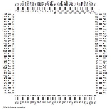 Specifications
Supply voltage range, VCC . . . . . . . . . . . . . . . . . . . . . . . . . . . . . . . . . . . . . . . . . . . . . . . . . . . . 0.5 V to 7 V
Input voltage range, VI (see Note 1) . . . . . . . . . . . . . . . . . . . . . . . . . . . . . . . . . . . . . 0.5 V to VCC + 0.5 V
Output voltage range, VO (see Note 1) . . . . . . . . . . . . . . . . . . . . . . . . . . . . . . . . . . . 0.5 V to VCC + 0.5 V
Input clamp current, IIK (VI < 0 or VI > VCC) . . . . . . . . . . . . . . . . . . . . . . . . . . . . .. . . . . . . . . . . . . . ±20 mA
Output clamp current, IOK (VO < 0 or VO > VCC) . . . . . . . . . . . . . . . . . . . . . . . . . . . . . . . . . . . . . . . ±50 mA
Continuous output current, IO (VO = 0 to VCC) . . . . . . . . . . . . . . . . . . . . . . . . . . . . . . . . .. . . . . . . . ±50 mA
Continuous current through VCC or GND . . . . . . . . . . . . . . . . . . . . . . . . . . . . . . . . . . . . .. . . . . . . . ±400 mA
Storage temperature range, Tstg . . . . . . . . . . . . . . . . . . . . . . . . . . . . . . . . . . . . . . . . . . . 65°C to 150°C
† Stresses beyond those listed under "absolute maximum ratings" may cause permanent damage to the device. These are stress ratings only, and functional operation of the device at these or any other conditions beyond those indicated under "recommended operating conditions" is not implied. Exposure to absolute-maximum-rated conditions for extended periods may affect device reliability.
NOTE 1: The input and output voltage ratings may be exceeded provided the input and output current ratings are observed.
DescriptionThe SN54ACT3632 is a high-speed, low-power CMOS clocked bidirectional FIFO memory. SN54ACT3632 supports clock frequencies up to 50 MHz and has read access times as fast as 11 ns. Two independent 512 * 36 dual-port SRAM FIFOs on the chip buffer data in opposite directions. Each FIFO SN54ACT3632 has flags to indicate empty and full conditions and two programmable flags (almost full and almost empty) to indicate when a selected number of words is stored in memory. Communication between each port can bypass the FIFO SN54ACT3632 via two 36-bit mailbox registers. Each mailbox register has a flag to signal when new mail has been stored. Two or more devices can be used in parallel to create wider data paths.
The SN54ACT3632 is a clocked FIFO, which means each port employs a synchronous interface. All data transfers through a port are gated to the low-to-high transition of a port clock by enable signals. The clocks for each port are independent of one another and can be asynchronous or coincident. The SN54ACT3632 enables for each port are arranged to provide a simple bidirectional interface between microprocessors and/or buses with synchronous control.
The input-ready (IRA, IRB) flag and almost-full (AFA, AFB) flag of a FIFO SN54ACT3632 are two-stage synchronized to the port clock that writes data to its array. The output-ready (ORA, ORB) flag and almost-empty (AEA, AEB) flag of a FIFO SN54ACT3632 are two-stage synchronized to the port clock that reads data from its array. Offset values for the almost-full and almost-empty flags of both FIFOs can be programmed from port A.
The SN54ACT3632 is characterized for operation over the full military temperature range of 55°C to 125°C.
For more information on SN54ACT3632 family, see the following application reports:
` FIFO Mailbox-Bypass Registers: Using Bypass Registers to Initialize DMA Control (literature number SCAA007)
` Interfacing TI Clocked FIFOs With TI Floating-Point Digital Signal Processors (literature number SCAA005)
` Metastability Performance of Clocked FIFOs (literature number SCZA004)

 SN54ACT3632 Data Sheet


