Features: · Free-Running CLKA and CLKB Can Be Asynchronous or Coincident· Clocked FIFO Buffering Data From Port A to Port B· Memory Size: 1024 × 36· Synchronous Read-Retransmit Capability· Mailbox Register in Each Direction· Programmable Almost-Full and Almost-Empty Flags· Microprocessor Interface...
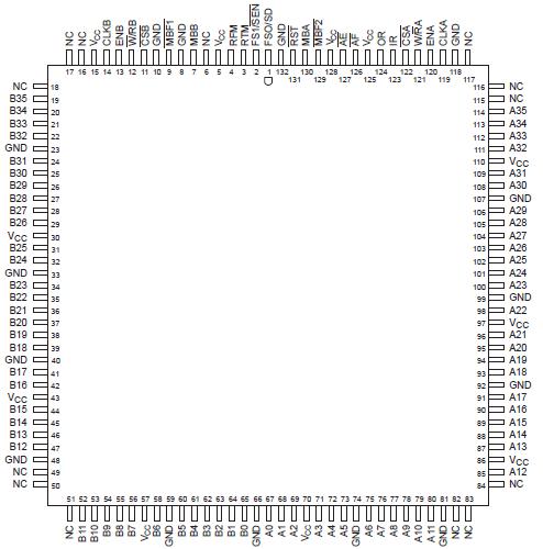
SN54ACT3641: Features: · Free-Running CLKA and CLKB Can Be Asynchronous or Coincident· Clocked FIFO Buffering Data From Port A to Port B· Memory Size: 1024 × 36· Synchronous Read-Retransmit Capability· Mailbox R...
SeekIC Buyer Protection PLUS - newly updated for 2013!
268 Transactions
All payment methods are secure and covered by SeekIC Buyer Protection PLUS.
Features: PinoutSpecificationsDescriptionThe SN54/74LS147 and SN54/74LS148 are Priority Encoders. ...
PinoutDescriptionThe LS155 and LS156 are Dual 1-of-4 Decoder/Demultiplexers with common Address in...

Supply voltage range, VCC . . . . . . . . . . . . . . . . . . . . . . . . . . . . . . . . . . . . . . . . . . . . . . . . . . 0.5 V to 7 V
Input voltage range, VI (see Note 1) . . . . . . . . . . . . . . . . . . . . . . . . . . . . . . . . . . . 0.5 V to VCC + 0.5 V
Output voltage range, VO (see Note 1) . . . . . . . . . . . . . . . . . . . . . . . . . . . . . . . .. . 0.5 V to VCC + 0.5 V
Input clamp current, IIK (VI < 0 or VI > VCC) . . . . . . . . . . . . . . . . . . . . . . . . . . . . . . . . . . . . . . . . ±20 mA
Output clamp current, IOK (VO < 0 or VO > VCC) . . . . . . . . . . . . . . . . . . . . . . . . . . . . . . . . . . . . . ±50 mA
Continuous output current, IO (VO = 0 to VCC) . . . . . . . . . . . . . . . . . . . . . . . . . . . . . . . . . . . . . . ±50 mA
Continuous current through VCC or GND . . . . . . . . . . . . . . . . . . . . . . . . . . . . . . . . . . . . . . . . . . ±400 mA
Storage temperature range, Tstg . . . . . . . . . . . . . . . . . . . . . . . . . . . . . . . . . . . . . . . . 65°C to 150°C
† Stresses beyond those listed under "absolute maximum ratings" may cause permanent damage to the device. These are stress ratings only, and functional operation of the device at these or any other conditions beyond those indicated under "recommended operating conditions" is not implied. Exposure to absolute-maximum-rated conditions for extended periods may affect device reliability.
NOTE 1: The input and output voltage ratings may be exceeded provided the input and output current ratings are observed.
The SN54ACT3641 is a high-speed, low-power, CMOS clocked FIFO memory. It supports clock frequencies up to 50 MHz and has read access times as fast as 15 ns. The 1024 * 36 dual-port SRAM FIFO buffers data from port A to port B. The FIFO memory has retransmit capability, SN54ACT3641 allows previously read data to be accessed again. The FIFO has flags to indicate empty and full conditions and two programmable flags (almost full and almost empty) to indicate when a selected number of words is stored in memory. Communication between each port of SN54ACT3641 can take place with two 36-bit mailbox registers. Each mailbox register has a flag to signal when new mail has been stored. Two or more devices can be used in parallel to create wider datapaths. Expansion is also possible in word depth.
The SN54ACT3641 is a clocked FIFO, which means each port employs a synchronous interface. All data transfers through a port are gated to the low-to-high transition of a continuous (free-running) port clock by enable signals. The continuous clocks for each port are independent of one another and can be asynchronous or coincident. The SN54ACT3641 enables for each port are arranged to provide a simple interface between microprocessors and/or buses with synchronous control.
The input-ready (IR) flag and almost-full (AF) flag of the FIFO SN54ACT3641 are two-stage synchronized to CLKA. The output-ready (OR) flag and almost-empty (AE) flag of the FIFO are two-stage synchronized to CLKB. Offset values for the AF and AE flags of the FIFO SN54ACT3641 can be programmed from port A or through a serial input.
The SN54ACT3641 is characterized for operation over the full military temperature range of 55°C to 125°C.
For more information on SN54ACT3641 family, see the following application reports:
• FIFO Patented Synchronous Retransmit: Programmable DSP-Interface Application for FIR Filtering (literature number SCAA009)
• FIFO Mailbox-Bypass Registers: Using Bypass Registers to Initialize DMA Control (literature number SCAA007)
• Metastability Performance of Clocked FIFOs (literature number SCZA004)