Features: ` Inputs Are TTL-Voltage Compatible
` EPIC E (Enhanced-Performance Implanted CMOS) 1-m Process
` Package Options Include Plastic Small-Outline (D), Shrink Small-Outline (DB), and Thin Shrink Small-Outline (PW) Packages, Ceramic Chip Carriers (FK) and Flatpacks (W), and Standard Plastic (N) and Ceramic (J) DIPS
Pinout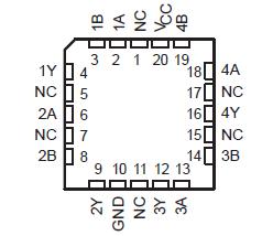 Specifications
Supply voltage range, VCC . . . . . . . . . . . . . . . . . . . . . . . . . . . . . . . . . . . . . . . . . . . . . 0.5 V to 7 V
Input voltage range, VI (see Note 1) . . . . . . . . . . . . . . . . . . . . . . .. . . . . . . . 0.5 V to VCC + 0.5 V
Output voltage range, VO (see Note 1) . . . . . . . . . . . . . . . . . . . . . . . . . . . . 0.5 V to VCC + 0.5 V
Input clamp current, IIK (VI < 0 or VI > VCC) . . . . . . . . . . . . . . . . . . . . . . . . . . . . . . . . . . . ±20 mA
Output clamp current, IOK (VO < 0 or VO > VCC) . . . . . . . . . . . . . . . . . . . . . . . . . . . . . . . . ±20 mA
Continuous output current, IO (VO = 0 to VCC) . . . . . . . . . . . . . . . . . . . . . . . . . . . . . . . . . ±50 mA
Continuous current through VCC or GND . . . . . . . . . . . . . . . . . . . . . . . . . . . . . . . . . . . . . .±200 mA
Maximum power dissipation at TA = 55°C (in still air) (see Note 2): D package . . . . . . . . . .1.25 W
DB package . . . . . . . . . . 0.5 W
N package . . . . . . . . . . . 1.1 W
PW package . . . . . . . . .. 0.5 W
Storage temperature range, Tstg . . . . . . . . . . . . . . . . . . . . . . . . . . . . . . . . . . . . 65°C to 150°C
† Stresses beyond those listed under "absolute maximum ratings" may cause permanent damage to the device. These are stress ratings only, and functional operation of the device at these or any other conditions beyond those indicated under "recommended operating conditions" is not implied. Exposure to absolute-maximum-rated conditions for extended periods may affect device reliability.
NOTES: 1. The input and output voltage ratings may be exceeded if the input and output current ratings are observed.
2. The maximum package power dissipation is calculated using a junction temperature of 150°C and a board trace length of 750 mils, except for the N package, which has a trace length of zero.
DescriptionThe SN54ACT86 are quadruple 2-input exclusive-OR gates. The devices perform the Boolean functions Y = A B or Y = AB + AB in positive logic.
A common application of SN54ACT86 is as a true/complement element. If one of the inputs is low, the other input is reproduced in true form at the output. If one of
the inputs is high, the signal on the other input is reproduced inverted at the output.
The SN54ACT86 is characterized for operation over the full military temperature range of 55°C to 125°C. The SN74ACT86 is characterized for operation from 40°C to 85°C.

 SN54ACT86 Data Sheet


