Features: ` EPICTM (Enhanced-Performance Implanted CMOS) Process
` Operating Range 2-V to 5.5-V VCC
` Contain Six Flip-Flops With Single-Rail Outputs
` Applications Include:
Buffer/Storage Registers
Shift Registers
Pattern Generators
` Latch-Up Performance Exceeds 250 mA Per JESD 17
` ESD Protection Exceeds JESD 22
2000-V Human-Body Model (A114-A)
200-V Machine Model (A115-A)
1000-V Charged-Device Model (C101)
` Package Options Include Plastic Small-Outline (D), Shrink Small-Outline (DB), Thin Very Small-Outline (DGV), Thin Shrink Small-Outline (PW), and Ceramic Flat (W) Packages, Ceramic Chip Carriers (FK), and Standard Plastic (N) and Ceramic (J) DIPs
Pinout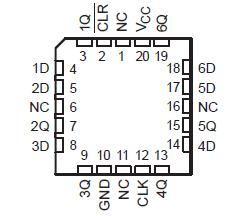 Specifications
Supply voltage range, VCC . . . . . . . . . . . . . . . . . . . . . . . . . . . . . . . . . . . . . .. . . . 0.5 V to 7 V
Input voltage range, VI (see Note 1) . . . . . . . . . . . . . . . . . . . . . . . . . . . . . . . . . 0.5 V to 7 V
Output voltage range, VO (see Note 1) . . . . . . . . . . . . . . . . . . . . . . . . . 0.5 V to VCC + 0.5 V
Input clamp current, IIK (VI < 0) . . . . . . . . . . . . . . . . . . . . . . .. . . . . . . . . . . . . . . . . . . 20 mA
Output clamp current, IOK (VO < 0 or VO > VCC) . . . . . . . . . . . . . . . . . . . . . . . . . . . . . ±20 mA
Continuous output current, IO (VO = 0 to VCC) . . . . . . . . . . . . . . . . . . . . . . . . . . . . . . ±25 mA
Continuous current through VCC or GND . . . . . . . . . . . . . . . . . . . . . . . . . . . . . . . . . . . ±50 mA
Package thermal impedance, JA (see Note 2): D package . . . . . . . . . .. . . . . . . . . . . 73°C/W
DB package . . . . . . . . . . . . . . . . . . . 82°C/W
DGV package . . . . . . . . . . . . . . . . .. 120°C/W
N package . . . . . . . . . . . . . . . . . . .. . 67°C/W
PW package . . . . . . . . . . . . . . . . . . 108°C/W
Storage temperature range, Tstg . . . . . . . . . . . . . . . . . . . . . . . . . . . . . . . . . 65°C to 150°C
† Stresses beyond those listed under "absolute maximum ratings" may cause permanent damage to the device. These are stress ratings only, and functional operation of the device at these or any other conditions beyond those indicated under "recommended operating conditions" is not implied. Exposure to absolute-maximum-rated conditions for extended periods may affect device reliability.
NOTES: 1. The input and output voltage ratings may be exceeded if the input and output current ratings are observed.
2. The package thermal impedance is calculated in accordance with JESD 51.
DescriptionThe SN54AHC174 devices are positive-edge-triggered D-type flip-flops with a direct clear (CLR) input and are designed for 2-V to 5.5-V VCC operation.
Information at the data (D) inputs that meets the setup time requirements is transferred to the outputs of SN54AHC174 on the positive-going edge of the clock (CLK) pulse. Clock triggering occurs at a particular voltage level and SN54AHC174 is not directly related to the transition time of the positive-going edge of CLK. When CLK is at either the high or low level, the D input has no effect at the output.
The SN54AHC174 is characterized for operation over the full military temperature range of 55°C to 125°C. The SN74AHC174 is characterized for operation from 40°C to 85°C.

 SN54AHC174 Data Sheet


