SN54AHCT139

Features: ` Inputs Are TTL-Voltage Compatible` Designed Specifically for High-Speed Memory Decoders and Data-Transmission Systems` Incorporate Two Enable Inputs to Simplify Cascading and/or Data Reception` Latch-Up Performance Exceeds 250 mA Per JESD 17` ESD Protection Exceeds JESD 22 2000-V Human...

product image

SN54AHCT139 Picture
SeekIC No. : 004496504 Detail

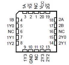
SN54AHCT139: Features: ` Inputs Are TTL-Voltage Compatible` Designed Specifically for High-Speed Memory Decoders and Data-Transmission Systems` Incorporate Two Enable Inputs to Simplify Cascading and/or Data Rec...

floor Price/Ceiling Price

Part Number:
SN54AHCT139
Supply Ability:
5000

Price Break

  • Qty
  • 1~5000
  • Unit Price
  • Negotiable
  • Processing time
  • 15 Days
Total Cost: $ 0.00

SeekIC Buyer Protection PLUS - newly updated for 2013!

  • Escrow Protection.
  • Guaranteed refunds.
  • Secure payments.
  • Learn more >>

Month Sales

268 Transactions

Rating

evaluate  (4.8 stars)

Upload time: 2025/12/24

Payment Methods

All payment methods are secure and covered by SeekIC Buyer Protection PLUS.

Notice: When you place an order, your payment is made to SeekIC and not to your seller. SeekIC only pays the seller after confirming you have received your order. We will also never share your payment details with your seller.
Product Details

Description


Features:

` Inputs Are TTL-Voltage Compatible
` Designed Specifically for High-Speed Memory Decoders and Data-Transmission Systems
` Incorporate Two Enable Inputs to Simplify Cascading and/or Data Reception
` Latch-Up Performance Exceeds 250 mA Per JESD 17
` ESD Protection Exceeds JESD 22
    2000-V Human-Body Model (A114-A)
   200-V Machine Model (A115-A)
   1000-V Charged-Device Model (C101)


Pinout

  Connection Diagram


Specifications

Supply voltage range, VCC . . . . . . . . . . . . . . . . . . . . . . . . . . . . . . . . . . . . . . . . . 0.5 V to 7 V
Input voltage range, VI (see Note 1) . . . . . . . . . . . . . . . . . . .. . . . . . . . . . . . . . . 0.5 V to 7 V
Output voltage range, VO (see Note 1) . . . . . . . . . . . . . . . . . .. . . . . . . 0.5 V to VCC + 0.5 V
Input clamp current, IIK (VI < 0) . . . . . . . . . . . . . . . . . . . . . . . . . . . . . . . . . . . . . . . . . 20 mA
Output clamp current, IOK (VO < 0 or VO > VCC) . . . . . . . . . . .. . . . . . . . . . . . . . . . . . ±20 mA
Continuous output current, IO (VO = 0 to VCC) . . . . . . . . . . .. . . . . . . . . . . . . . . . . . . ±25 mA
Continuous current through VCC or GND . . . . . . . . . . . . . . . .. . . . . . . . . . . . . . . . . . . ±75 mA
Package thermal impedance, JA (see Note 2): D package . . . .. . . . . . . . . . . . . . . . . 73°C/W
                                                                          DB package . . . . . . . . . . . . . . . . . . . . 82°C/W
                                                                          DGV package . . . . . . . . . . . . . . . . . . 120°C/W
                                                                          N package . . . . . . .  . . . . . . . . . . . . . . 67°C/W
                                                                          NS package . . . . . . .  . . . . . . . . . . . . . 64°C/W
                                                                          PW package . . . . . . . . . . . . . . . . . . . 108°C/W
Storage temperature range, Tstg . . . . . . . . . . . . . . . . . . . . .. . . . . . . . . . . . . 65°C to 150°C

† Stresses beyond those listed under "absolute maximum ratings" may cause permanent damage to the device. These are stress ratings only, and functional operation of the device at these or any other conditions beyond those indicated under "recommended operating conditions" is not implied. Exposure to absolute-maximum-rated conditions for extended periods may affect device reliability.
NOTES: 1. The input and output voltage ratings may be exceeded if the input and output current ratings are observed.
             2. The package thermal impedance is calculated in accordance with JESD 51-7.


Description

The SN54AHCT139 is dual 2-line to 4-line decoders/demultiplexers designed for 4.5-V to 5.5-V VCC operation. These devices are designed to be used in high-performance memory-decoding or data-routing applications requiring very short propagation delay times. In high-performance memory systems, SN54AHCT139 can be used to minimize the effects of system decoding. When used with high-speed memories utilizing a fast enable circuit, the delay times of these decoders and the enable time of the memory usually are less than the typical access time of the memory. This means that the effective system delay introduced by the decoders is negligible.


Customers Who Bought This Item Also Bought

Margin,quality,low-cost products with low minimum orders. Secure your online payments with SeekIC Buyer Protection.
Resistors
Tapes, Adhesives
803
RF and RFID
Crystals and Oscillators
Boxes, Enclosures, Racks
View more