Features: `State-of-the-Art Advanced BiCMOS Technology (ABT) Widebus Design for 2.5-V and 3.3-V Operation and Low
`Static-Power Dissipation
`Support Mixed-Mode Signal Operation (5-V Input and Output Voltages With 2.3-V to 3.6-V VCC)
`Typical VOLP (Output Ground Bounce) <0.8 V at VCC = 3.3 V, TA = 25°C
`High Drive (12/12 mA at 3.3-V VCC)
`Ioff and Power-Up 3-State Support Hot Insertion
`Use Bus Hold on Data Inputs in Place of
`External Pullup/Pulldown Resistors to
`Prevent the Bus From Floating
`Output Ports Have Equivalent 30-Ω Series
`Resistors, So No External Resistors Are Required
`Flow-Through Architecture Facilitates
`Printed Circuit Board Layout
`Distributed VCC and GND Pins Minimize
`High-Speed Switching Noise
`Latch-Up Performance Exceeds 100 mA Per
`JESD 78, Class II
`ESD Protection Exceeds JESD 22
2000-V Human-Body Model (A114-A)
200-V Machine Model (A115-A)
1000-V Charged-Device Model (C101)Pinout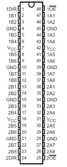 SpecificationsSupply voltage range, . . . . . . . . . . . . . . . . . . . . . . . . . . . . . . . . . . . . . . . . . . . . . .VCC 0.5 V to 4.6 V
Input voltage range, VI (see Note 1) . . . . . . . . . . . . . . . . . . . . . . . . . . . . . . . . . . . . . . ..0.5 V to 7 V
Voltage range applied to any output in the high or power-off state, VO (see Note 1) . . 0.5 V to 7 V
Output current in the low state, IO: SN54ALVTHR16245 . . . . . . . . . . . . . . . . . . . . . . . . . . . . . . .96 mA
SN74ALVTHR16245 . . . . . . . . . . . . . . . . . . . . . . . . . . . . . . . . . . . . .. .. .. .. .. .. .. .. .. .. .. .. .. .. ..128 mA
Output current in the high state, IO: SN54ALVTHR16245 . . . . . . . . . . . . . . . . . . . . . . . . . . . . .48 mA
SN74ALVTHR16245 . . . . . . . . . . . . . . . . . . . . . . . . . . . . . . . . . . . . .. .. .. .. .. .. .. .. .. .. .. .. .. .. .64 mA
Input clamp current, . . . . . . . . . . . . . . . . . . . . . . . . . . . . . . . . . . . . . . . . . . . . . . . .IIK (VI < 0) 50 mA
Output clamp current, . . . . . . . . . . . . . . . . . . . . . . . . . . . . . . . . . . . . . . . . . . . . . .IOK (VO < 0) 50 mA
Package thermal impedance, JA (see Note 2): DGG package . . . . . . . . . . . . . . . . . . . . . . . .. 70°C/W
DGV package . . . . . . . . . . . . . . . . . . . . . . . . . . . . . . . . .. .. .. .. .. .. .. .. .. .. .. .. .. .. .. .. .. .. .. .. .58°C/W
DL package . . . . . . . . . . . . . . . . . . . . . . . . . . . . . . . .. .. .. .. .. .. .. .. .. .. .. .. .. .. .. .. .. .. .. .. .. ...63°C/W
GQL package . . . . . . . . . . . . . . . . . . . . . . . . . . . . . .. .. .. .. .. .. .. .. .. .. .. .. .. .. .. .. .. .. .. .. .. .. ..42°C/W
Storage temperature range, Tstg . . . . . . . . . . . . . . . . . . . . . . . . . . . . . . . . . . . . . . . . 65°C to 150°C
Stresses beyond those listed under "absolute maximum ratings" may cause permanent damage to the device. These are stress ratings only, and functional operation of the device at these or any other conditions beyond those indicated under "recommended operating conditions" is not implied. Exposure to absolute-maximum-rated conditions for extended periods may affect device reliability.
NOTES: 1. The input and output negative-voltage ratings may be exceeded if the input and output clamp-current ratings are observed.
2. The package thermal impedance is calculated in accordance with JESD 51-7.
DescriptionSN54ALVTHR16245 can be used as two 8-bit transceivers or one 16-bit transceiver. They allow data transmission from the A bus to the B bus or from the B bus to the A bus, depending on the logic level at the direction-control (DIR) input. The output-enable (OE) input of SN54ALVTHR16245 can be used to disable the device so that the buses are effectively isolated.
All outputs of SN54ALVTHR16245 are designed to sink up to 12 mA, and include equivalent 30-Ω resistors to reduce overshoot and undershoot.
SN54ALVTHR16245 is fully specified for hot-insertion applications using Ioff and power-up 3-state. The Ioff circuitry disables the outputs, preventing damaging current backflow through the device when SN54ALVTHR16245 is powered down. The power-up 3-state circuitry places the outputs in the high-impedance state during power up and power down, which prevents driver conflict.
Active bus-hold circuitry of SN54ALVTHR16245 is provided to hold unused or floating data inputs at a valid logic level. Use of pullup or pulldown resistors with the bus-hold circuitry is not recommended.
When VCC is between 0 and 1.2 V, the SN54ALVTHR16245 is in the high-impedance state during power up or power down. However, to ensure the high-impedance state above 1.2 V, OE should be tied to VCC through a pullup resistor; the minimum value of the resistor SN54ALVTHR16245 is determined by the current-sinking capability of the driver.

 SN54ALVTHR16245 Data Sheet


