Features: • Open-Collector Version of 4BCT244
• Open-Collector Outputs Drive Bus Lines or Buffer Memory Address Registers
• ESD Protection Exceeds 2000 V Per MIL-STD-883C Method 3015
• Packages Options Include Plastic Small-Outline (DW) Packages, Ceramic Chip Carriers (FK) and Flatpacks (W), and Standard Plastic and Ceramic 300-mil DIPs (J, N)
Pinout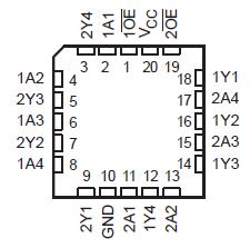 Specifications
Supply voltage range, VCC . . . . . . . . . . . . . . . . . . . . . . . . . . . . . . . . . . . . . . . . . . . . . . 0.5 V to 7 V
Input voltage range, VI (see Note 1) . . . . . . . . . . . . . . . . . . . . . . . . .. . . . . . . . . . . . . . 0.5 V to 7 V
Input current range, II . . . . . . . . . . . . . . . . . . . . . . . . . . . . . . . . . . . . . .. . . . . . . . . . 30 mA to 5 mA
Voltage range applied to any output in the disabled or power-off state, VO . . . . .. . 0.5 V to 5.5 V
Voltage range applied to any output in the high state, VO . . . . . . . . . . . . . . . . . . . . . 0.5 V to VCC
Current into any output in the low state: SN54BCT760 . . . . . . . . . . . . . . . . . . . . . . . . . . . . . . 96 mA
SN74BCT760 . . . . . . . . . . . . . . . . . .. . . . . . . . . . . . 128 mA
Operating free-air temperature range: SN54BCT760 . . . . . . . . . . . . . . . . . . . .. . . 55°C to 125°C
SN74BCT760 . . . . . . . . . . . . . . . . . . . .. . . . . . . 0°C to 70°C
Storage temperature range . . . . . . . . . . . . . . . . . . . . . . . . . . . . . . . . . . . .. . . . . . 65°C to 150°C
‡ Stresses beyond those listed under "absolute maximum ratings" may cause permanent damage to the device. These are stress ratings only, and
functional operation of the device at these or any other conditions beyond those indicated under "recommended operating conditions" is not implied. Exposure to absolute-maximum-rated conditions for extended periods may affect device reliability.
NOTE 1: The negative input voltage rating may be exceeded if the input clamp current rating is observed.
DescriptionThese octal buffers and line drivers of SN54BCT760 are designed specifically to improve both the performance and density of 3-state memory address drivers, clock
drivers, and bus-oriented receivers and transmitters.
The SN54BCT760 is organized as two 4-bit buffers/line drivers with separate output-enable (OE) inputs. When OE is low, the SN54BCT760 passes data from the A inputs to the Y outputs. When OE is high, the outputs are in the high-impedance state.
The SN54BCT760 is characterized for operation over the full military temperature range of 55°C to 125°C. The SN74BCT760 is characterized for operation from 0°C to 70°C.

 SN54BCT760 Data Sheet


