SN54F299

Features: • Four Modes of Operation: Hold (Store) Shift Right Shift Left Load Data• Operates With Outputs Enabled or at High Impedance• 3-State Outputs Drive Bus Lines Directly• Can Be Cascaded for N-Bit Word Lengths• Direct Overriding Clear• Applications: Stack...

product image

SN54F299 Picture
SeekIC No. : 004496798 Detail

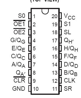
SN54F299: Features: • Four Modes of Operation: Hold (Store) Shift Right Shift Left Load Data• Operates With Outputs Enabled or at High Impedance• 3-State Outputs Drive Bus Lines DirectlyR...

floor Price/Ceiling Price

Part Number:
SN54F299
Supply Ability:
5000

Price Break

  • Qty
  • 1~5000
  • Unit Price
  • Negotiable
  • Processing time
  • 15 Days
Total Cost: $ 0.00

SeekIC Buyer Protection PLUS - newly updated for 2013!

  • Escrow Protection.
  • Guaranteed refunds.
  • Secure payments.
  • Learn more >>

Month Sales

268 Transactions

Rating

evaluate  (4.8 stars)

Upload time: 2025/12/24

Payment Methods

All payment methods are secure and covered by SeekIC Buyer Protection PLUS.

Notice: When you place an order, your payment is made to SeekIC and not to your seller. SeekIC only pays the seller after confirming you have received your order. We will also never share your payment details with your seller.
Product Details

Description


Features:

• Four Modes of Operation:
  Hold (Store)
  Shift Right
  Shift Left
  Load Data
• Operates With Outputs Enabled or at High Impedance
• 3-State Outputs Drive Bus Lines Directly
• Can Be Cascaded for N-Bit Word Lengths
• Direct Overriding Clear
• Applications:
  Stacked or Push-Down Registers
  Buffer Storage
  Accumulator Registers
• Package Options Include Plastic
  Small-Outline Packages, Ceramic Chip
  Carriers, and Standard Plastic and Ceramic 300-mil DIPs


Pinout

  Connection Diagram


Specifications

Supply voltage range, VCC . . . . . . . . . . . . . . . . . . . . . . . . . . . . . . . . . . . . . . . . . . . . . . . . . . . . 0.5 V to 7 V
Input voltage range, VI (see Note 1) . . . . . . . . . . . . . . . . . . . . . . . . . . . . . . . . . . . . . . . . . . . . .1.2 V to 7 V
Input current range . . . . . . . . . . . . . . . . . . . . . . . . . . . . . . . . . . . . . . . . . . . . . . . . . . . . . . . .30 mA to 5 mA
Voltage range applied to any output in the disabled or power-off state . . . . . . . . . . . . . . . . 0.5 V to 5.5 V
Voltage range applied to any output in the high state . . . . . . . . . . . . . . . . . . . . . . . . . . . . . . .0.5 V to VCC
Current into any output in the low state: QA4 or QH4 . . . . . . . . . . . . . . . . . . . . . . . . . . . . . . . . . . . . .40 mA
SN54F299 (QA thru QH) . . . . . . . . . . . . . . . . . . . . . . . . . . . . . . . . . . . . . . . . . . . . . . . . . . . . . . . . . . . .40 mA
SN74F299 (QA thru QH) . . . . . . . . . . . . . . . . . . . . . . . . . . . . . . . . . . . . . . . . . . . . . . . . . . . . . . . . . . . .48 mA
Operating free-air temperature range: SN54F299 . . . . . . . . . . . . . . . . . . . . . . . . . . . . . . . . 55°C to 125°C
SN74F299 . . . . . . . . . . . . . . . . . . . . . . . . . . . . . . . . . . . . . . . . . . . . . . . . . . . . . . . . . . . . . . .. . . 0°C to 70°C
Storage temperature range . . . . . . . . . . . . . . . . . . . . . . . . . . . . . . . . . . . . . . . . . . . . . . . . . . 65°C to 150°C
‡ Stresses beyond those listed under "absolute maximum ratings" may cause permanent damage to the device. These are stress ratings only and
functional operation of the device at these or any other conditions beyond those indicated under "recommended operating conditions" is not
implied. Exposure to absolute-maximum-rated conditions for extended periods may affect device reliability.
NOTE 1: The input voltage ratings may be exceeded provided the input current ratings are observed.


Description

These 8-bit universal shift/storage registers of SN54F299 feature multiplexed I/O ports to achieve full 8-bit data handling in a single 20-pin package. Two function-select (S0, S1) inputs and two output-enable (OE1, OE2) inputs of SN54F299 can be used to choose the modes of operation listed in the function table.

Synchronous parallel loading of SN54F299 is accomplished by taking both S0 and S1 high. This places the 3-state outputs in a high-impedance state and permits data that is applied on the I/O ports to be clocked into the register. Reading out of the register can be ccomplished while the outputs of SN54F299 are enabled in any mode. Clearing occurs when the clear (CLR) input is low.
Taking either OE1 or OE2 high disables the outputs but has no effect on clearing, shifting, or storage of data.

The SN54F299 is characterized for operation over the full military temperature range of 55°C to 125°C. The N74F299 is characterized for operation from 0°C to 70°C.


Customers Who Bought This Item Also Bought

Margin,quality,low-cost products with low minimum orders. Secure your online payments with SeekIC Buyer Protection.
Memory Cards, Modules
Optoelectronics
Computers, Office - Components, Accessories
Discrete Semiconductor Products
LED Products
View more