SN54FB2040

Features: Compatible With IEEE Std 1194.1-1991 (BTL)TTL A Port, Backplane Transceiver Logic (BTL) B PortOpen-Collector B-Port Outputs Sink 100 mAIsolated Logic-Ground and Bus-Ground Pins Reduce NoiseHigh-Impedance State During Power Up and Power DownBIAS VCC Pin Minimizes Signal Distortion During ...

product image

SN54FB2040 Picture
SeekIC No. : 004496813 Detail

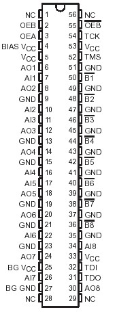
SN54FB2040: Features: Compatible With IEEE Std 1194.1-1991 (BTL)TTL A Port, Backplane Transceiver Logic (BTL) B PortOpen-Collector B-Port Outputs Sink 100 mAIsolated Logic-Ground and Bus-Ground Pins Reduce Nois...

floor Price/Ceiling Price

Part Number:
SN54FB2040
Supply Ability:
5000

Price Break

  • Qty
  • 1~5000
  • Unit Price
  • Negotiable
  • Processing time
  • 15 Days
Total Cost: $ 0.00

SeekIC Buyer Protection PLUS - newly updated for 2013!

  • Escrow Protection.
  • Guaranteed refunds.
  • Secure payments.
  • Learn more >>

Month Sales

268 Transactions

Rating

evaluate  (4.8 stars)

Upload time: 2025/12/24

Payment Methods

All payment methods are secure and covered by SeekIC Buyer Protection PLUS.

Notice: When you place an order, your payment is made to SeekIC and not to your seller. SeekIC only pays the seller after confirming you have received your order. We will also never share your payment details with your seller.
Product Details

Description


Features:

 Compatible With IEEE Std 1194.1-1991 (BTL)
 TTL A Port, Backplane Transceiver Logic (BTL) B Port
 Open-Collector B-Port Outputs Sink 100 mA
 Isolated Logic-Ground and Bus-Ground Pins Reduce Noise
 High-Impedance State During Power Up and Power Down
 BIAS VCC Pin Minimizes Signal Distortion During Live Insertion or Withdrawal
 B-Port Biasing Network Preconditions the Connector and PC Trace to the BTL High-Level Voltage
 Package Options Include Plastic Quad Flat (RC) and Ceramic Flat (WD) Packages


Pinout

  Connection Diagram


Specifications

Supply voltage range, VCC  . . . . . . . . . . . . . . . . . . . . . . . . . . . . . . . . . . . . . . .  . . . . . . . . .0.5 V to 7 V
Input voltage range, VI: Except B port  . . . . . . . . . . . . . . . . . . . . . . . . . . . . .. . . . . . . . . . .1.2 V to 7 V
                                       B port . . . . . . . . . . . . . . . . . . . . . . . . . . . . . . . . . . .. . . . . . . . . .1.2 V to 3.5 V
Voltage range applied to any B output in the disabled or power-off state, VO  . . . . . . . .0.5 V to 3.5 V
Voltage range applied to any output in the high state, VO: A port . . . . . . . .  . . .  . . . . . . . 0.5 V to VCC
Input clamp current, IIK: Except B port . . . . . . . . . . . . . . . . . . . . . . . . . . . . . . . . .. . . . . . . . .. . . .40 mA
                                        B port . . . . . . . . . . . . . . . . . . . . . . . . . . . . . . . . . . . .  . . . . . . . . . . .. . . 18 mA
Current applied to any single output in the low state, IO: A port  . . . . . . . . . . . . .  . . . . . . . .  . . . .48 mA
                                                                                           B port  . . . . . . . . . . . . . .. . . . . . . .  . . .200 mA
Package thermal impedance, JA (see Note 1)  . . . . . . . . . . . . . . . . . . . . . . . . . . . . . . . . . . . . . . .44°C/W
Storage temperature range, Tstg  . . . . . . . . . . . . . . . . . . . . . . . . . . . . . . . . . . . . . . . . . . .65°C to 150°C


Description

The SN54FB2040 is 8-bit transceivers designed to translate signals between TTL and backplane transceiver logic (BTL) environments.

The B port operates at BTL-signal levels. The open-collector B ports are specified to sink 100 mA. Two output enables (OEB and OEB) are provided for the B outputs. When OEB SN54FB2040 is high and OEB is low, the B port is active and reflects the inverse of the data present at the A-input pins. When OEB is low, OEB is high, or VCC is less than 2.1 V, the B port is turned off.

The A port operates at TTL-signal levels and has separate input and output pins. The A outputs reflect the inverse of the data at the B port when the A-port output enable (OEA) is high. When OEA is low or when VCC is less than 2.1 V, the A outputs are in the high-impedance state. Pins are allocated for the four-wire IEEE Std 1149.1 (JTAG) test bus. TMS and TCK are not connected, and TDI is shorted to TDO.

BIAS VCC establishes a voltage between 1.62 V and 2.1 V on the BTL outputs when VCC is not connected.

The SN54FB2040 is characterized for operation over the full military temperature range of 55°C to 125°C. The SN74FB2040 is characterized for operation from 0°C to 70°C.


Customers Who Bought This Item Also Bought

Margin,quality,low-cost products with low minimum orders. Secure your online payments with SeekIC Buyer Protection.
Batteries, Chargers, Holders
Undefined Category
Circuit Protection
Inductors, Coils, Chokes
Tapes, Adhesives
803
Power Supplies - Board Mount
View more