Features: Members of the Texas Instruments Widebus
TM Family
Universal Bus Transceiver (UBTTM) Combines D-Type Latches and D-Type Flip-Flops for Operation in Transparent, Latched, Clocked, or Clock-Enabled Modes
Translate Between GTL/GTL+ Signal Levels and LVTTL Logic Levels
Support Mixed-Mode (3.3-V and 5-V) Signal Operation on A-Port and Control Inputs
B-Port Transition Time Optimized for Distributed Backplane Loads
Ioff Supports Partial-Power-Down Mode Operation
Bus Hold on A-Port Inputs Eliminates the Need for External Pullup/Pulldown Resistors
Distributed VCC and GND-Pin Configuration Minimizes High-Speed Switching Noise
ESD Protection Exceeds JESD 22
2000-V Human-Body Model (A114-A)
200-V Machine Model (A115-A)
1000-V Charged-Device Model (C101)
Latch-Up Performance Exceeds 100 mA Per JESD 78, Class II
Package Options Include Plastic Shrink Small-Outline (DL), Thin Shrink Small-Outline (DGG), and Ceramic Flat (WD) PackagesPinout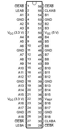 Specifications
| |
MIN MAX |
UNIT |
VCC Supply voltage range
|
3.3 V |
-0.5 4.6 |
V |
| 5 V |
-0.5 7 |
VI Input voltage range(2)
|
A-port and control inputs |
-0.5 7 |
V |
B port and VREF
|
-0.5 4.6 |
Voltage range applied to any output
VO in the high or power-off state(2) |
A port |
-0.5 7 |
V |
| B port |
-0.5 4.6 |
IO Current into any output in the low state
|
A port |
128 |
mA |
| B port |
80 |
IO Current into any A-port output in the high state(3)
|
64 |
mA |
Continuous current through each VCC or GND
|
|
-100 |
mA |
| IIK Input clamp current |
VI < 0 |
-50 |
mA |
| IOK Output clamp current |
VO < 0
|
-50 |
mA |
JA Package thermal impedance(4)
|
DGG package |
64 |
/W |
| DL package |
56 |
Tstg Storage temperature range
|
|
-65 150 |
|
Description The SN54GTL16612A devices are 18-bit universal bus transceivers (UBT) that provide LVTTL-to-GTL+and GTL+-to-LVTTL signal-level translation. They allow for transparent, latched, clocked, or clock-enabled modes of data transfer. SN54GTL16612A provides a high-speed interface between cards operating at LVTTL logic levels and backplanes operating at GTL+ signal levels. High-speed(about two times faster than standard LVTTL or TTL) backplane operation is a direct result of the reduced output swing (<1 V), reduced input threshold levels, and output edge control (OEC(TM)). Improved GTL+ OEC circuits minimize bus settling time and have been designed and tested using several backplane models.
Figure 1 shows actual SN54GTL16612A output waveforms using a synchronous clock at 75 MHz. The test backplane is a 16-slot, 14-inch board with loaded impedance of 33 ?. VTT is 1.5 V, VREF is 1 V, and RTT pullup resistor is 50 .The driver is in slot 8, with receivers in alternate slots 1, 3, 5, 7, 10, 12, 14, and 16. Receiver slot-1 signals are shown. The signal becomes progressively worse as the receiver moves closer to the driver or the spacing between receiver cards is reduced. The clock of SN54GTL16612A is independent of the data, and the system clock frequency is limited by the backplane flight time to about 80-90 MHz. This frequency can be increased even more (30% to 40%) if the clock of SN54GTL16612A is generated and transmitted together with the data from the driver card (source synchronous).

 SN54GTL16612A Data Sheet


