Features: ` Members of the Texas Instruments idebusE Family` D-Type Flip-Flops With Qualified Storage nable` Translate Between GTL/GTL+ Signal Levels d LVTTL Logic Levels` Support Mixed-Mode Signal Operation on l Ports (5-V Input/Output Voltages With3.3-V VCC)` Ioff Supports Partial-Power-Dow...
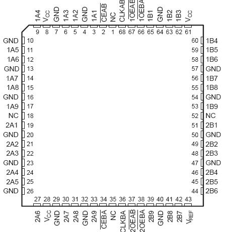
SN54GTL16923: Features: ` Members of the Texas Instruments idebusE Family` D-Type Flip-Flops With Qualified Storage nable` Translate Between GTL/GTL+ Signal Levels d LVTTL Logic Levels` Support Mixed-Mode Sig...
SeekIC Buyer Protection PLUS - newly updated for 2013!
268 Transactions
All payment methods are secure and covered by SeekIC Buyer Protection PLUS.
Features: PinoutSpecificationsDescriptionThe SN54/74LS147 and SN54/74LS148 are Priority Encoders. ...
PinoutDescriptionThe LS155 and LS156 are Dual 1-of-4 Decoder/Demultiplexers with common Address in...

The SN54GTL16923 is 18-bit registered bus transceivers that provide LVTTL-to-GTL/GTL+ and GTL/GTL+-to-LVTTL signal-level translation. They are partitioned as two 9-bit transceivers with individualoutput-enable controls and contain D-type flip-flops for temporary storage of data flowing in either direction. The SN54GTL16923 provides an interface between cards operating at LVTTL logic levels and a backplane operating at GTL/GTL+ signal levels. Higher-speed operation is a direct result of the reduced output swing (<1 V), reduced input threshold levels, and output edge control (OECE).
The user has the flexibility of using SN54GTL16923 at either GTL (VTT = 1.2 V and VREF = 0.8 V) or the preferred higher noise margin GTL+ (VTT = 1.5 V and VREF = 1 V) signal levels. GTL+ is the Texas Instruments derivative of the Gunning transceiver logic (GTL) JEDEC standard JESD 8-3. The B port normally operates at GTL or GTL+ signal levels, while the A-port and control inputs are compatible with LVTTL logic levels. All inputs can be driven from either 3.3-V or 5-V devices which allows use in a mixed 3.3-V/5-V system environment. VREF is the reference input voltage for the B port.
Data flow in each direction of SN54GTL16923 is controlled by the output-enable (OEAB and OEBA) and clock (CLKAB and CLKBA) inputs. The clock-enable (CEAB and CEBA) inputs are used to enable or disable the clock for all 18 bits at a time. However, OEAB and OEBA are designed to control each 9-bit transceiver independently, which makes the SN54GTL16923 more versatile.
For A-to-B data flow, the SN54GTL16923 operates on the low-to-high transition of CLKAB if CEAB is low. When OEAB is low, the outputs are active. When OEAB is high, the outputs of SN54GTL16923 are in the high-impedance state. Data flow for B to A is similar to that of A to B but uses OEBA, CLKBA, and CEBA.
SN54GTL16923 is fully specified for partial-power-down applications using Ioff. The Ioff circuitry disables the outputs, preventing damaging current backflow through the devices when they are powered down. Active bus-hold circuitry holds unused or undriven LVTTL inputs of SN54GTL16923 at a valid logic state. Use of pullup or pulldown resistors with the bus-hold circuitry is not recommended.
To ensure the high-impedance state during power up or power down, OE should be tied to VCC through a pullup resistor; the minimum value of the resistor SN54GTL16923 is determined by the current-sinking capability of the driver.
The SN54GTL16923 is characterized for operation over the full military temperature range of 55°C to 125°C. The SN74GTL16923 is characterized for operation from 40°C to 85°C.