Features: · Allow Design of Either RC or Crystal Oscillator Circuits
· Package Options Include Plastic Small-Outline (D) and Ceramic Flat (W) Packages, Ceramic Chip Carriers (FK), and Standard Plastic (N) and Ceramic (J) 300-mil DIPs
Pinout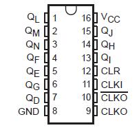 Specifications
Supply voltage range, VCC . . . . . . . . . . . . . . . . . . . . . . . . . . . . . . . . . . . . . . . 0.5 V to 7 V
Input clamp current, IIK (VI < 0 or VI > VCC) (see Note 1) . . . . . . . . . . . . . . . . . . . ±20 mA
Output clamp current, IOK (VO < 0 or VO > VCC) (see Note 1) . . . . . . . . . . . . . . . . ±20 mA
Continuous output current, IO (VO = 0 to VCC) . . . . . . . . . . . . . . . . . . . . . . . . . . . . ±25 mA
Continuous current through VCC or GND . . . . . . . . . . . . . . . . . . . . . . . . . . . . . . . . . ±50 mA
Package thermal impedance, JA (see Note 2): D package . . . . . . . . . . . . . . . . . 113°C/W
N package . . . . . . . . . . . . . . . . . . . 78°C/W
Storage temperature range, Tstg . . . . . . . . . . . . . . . . . . . . . . . . . . . . . . . 65°C to 150°C
† Stresses beyond those listed under "absolute maximum ratings" may cause permanent damage to the device. These are stress ratings only, and functional operation of the device at these or any other conditions beyond those indicated under "recommended operating conditions" is not implied. Exposure to absolute-maximum-rated conditions for extended periods may affect device reliability.
NOTES: 1. The input and output voltage ratings may be exceeded if the input and output current ratings are observed.
2. The package thermal impedance is calculated in accordance with JESD 51, except for through-hole packages, which use a trace length of zero.
DescriptionThe SN54HC4060 consist of an oscillator section and 14 ripple-carry binary counter stages. The oscillator configuration allows design of either RC or crystal-oscillator circuits. A high-to-low transition on the clock (CLKI) input increments the counter. A high level at the clear (CLR) input of SN54HC4060 disables the oscillator (CLKO goes high and CLKO goes low) and resets the counter to zero (all Q outputs low).
The SN54HC4060 is characterized for operation over the full military temperature range of 55°C to 125°C. The SN74HC4060 is characterized for operation from 40°C to 85°C.

 SN54HC4060 Data Sheet


