SN54HCT377

Features: `Operating Voltage Range of 4.5 V to 5.5 V`Outputs Can Drive Up To 10 LSTTL Loads`Low Power Consumption, 80-A Max ICC`Typical tpd = 12 ns`±4-mA Output Drive at 5 V`Low Input Current of 1 A Max`Inputs Are TTL-Voltage Compatible`Contain Eight Flip-Flops With Single-Rail Outputs`Clock Enabl...

product image

SN54HCT377 Picture
SeekIC No. : 004496937 Detail

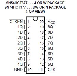
SN54HCT377: Features: `Operating Voltage Range of 4.5 V to 5.5 V`Outputs Can Drive Up To 10 LSTTL Loads`Low Power Consumption, 80-A Max ICC`Typical tpd = 12 ns`±4-mA Output Drive at 5 V`Low Input Current of 1 A...

floor Price/Ceiling Price

Part Number:
SN54HCT377
Supply Ability:
5000

Price Break

  • Qty
  • 1~5000
  • Unit Price
  • Negotiable
  • Processing time
  • 15 Days
Total Cost: $ 0.00

SeekIC Buyer Protection PLUS - newly updated for 2013!

  • Escrow Protection.
  • Guaranteed refunds.
  • Secure payments.
  • Learn more >>

Month Sales

268 Transactions

Rating

evaluate  (4.8 stars)

Upload time: 2025/12/24

Payment Methods

All payment methods are secure and covered by SeekIC Buyer Protection PLUS.

Notice: When you place an order, your payment is made to SeekIC and not to your seller. SeekIC only pays the seller after confirming you have received your order. We will also never share your payment details with your seller.
Product Details

Description


Features:

`Operating Voltage Range of 4.5 V to 5.5 V
`Outputs Can Drive Up To 10 LSTTL Loads
`Low Power Consumption, 80-A Max ICC
`Typical tpd = 12 ns
`±4-mA Output Drive at 5 V
`Low Input Current of 1 A Max
`Inputs Are TTL-Voltage Compatible
`Contain Eight Flip-Flops With Single-Rail
   Outputs
`Clock Enable Latched to Avoid False
   Clocking
`Applications Include:
   Buffer/Storage Registers
   Shift Registers
   Pattern Generators


Pinout

  Connection Diagram


Specifications

Supply voltage range, VCC . . . . . . . . . . . . . . . . . . . . . . . . . . . . . . . . . . . . . . . . . .. . . . . . . . . . . . 0.5 V to 7 V
Input clamp current, IIK (VI < 0 or VI > VCC) (see Note 1) . . . . . . . . . . . . . . . . . . . . .. . . . . . . . . . . . . ±20 mA
Output clamp current, IOK (VO < 0 or VO > VCC) (see Note 1) . . . . . . . . . . . . . . . . . . . . . . . . . . . . . . ±20 mA
Continuous output current, IO (VO = 0 to VCC) . . . . . . . . . . . . . . . . . . . . . . . . . . . . . . . . . . . . . . . . . . ±25 mA
Continuous current through VCC or GND . . . . . . . . . . . . . . . . . . . . . . . . . . . . . . . . .. . . . . . . . . . . . . . . ±50 mA
Package thermal impedance, JA (see Note 2): DW package . . . . . . . . . . . . . . . . . . . . . . . . . . . . . . . 58°C/W
                                                                      N package . . . . . . . . . . . . . . . . . . . . . . . . . . . . . . . . . . . 69°C/W
Storage temperature range, Tstg . . . . . . . . . . . . . . . . . . . . . . . . . . . . . . . . . . . . . . . . . . . . . 65°C to 150°C
† Stresses beyond those listed under "absolute maximum ratings" may cause permanent damage to the device. These are stress ratings only, and
functional operation of the device at these or any other conditions beyond those indicated under "recommended operating conditions" is not
implied. Exposure to absolute-maximum-rated conditions for extended periods may affect device reliability.
NOTES: 1. The input and output voltage ratings may be exceeded if the input and output current ratings are observed.
2. The package thermal impedance is calculated in accordance with JESD 51-7.


Description

These devices are positive-edge-triggered D-type flip-flops. The 'HCT377 devices are similar to the  HCT273 devices, but feature a latched clock-enable (CLKEN) input instead of a common clear.

Information at the data (D) inputs of HCT377 meeting the setup time requirements is transferred to the Q outputs on the positive-going edge of the clock (CLK) pulse if CLKEN is low. Clock triggering occurs at a particular voltage level and is not directly related to the transition time of the positive-going pulse. When CLK is at either the high or low level, the D input has no effect at the output. HCT377 is designed to prevent false clocking by transitions at CLKEN


Customers Who Bought This Item Also Bought

Margin,quality,low-cost products with low minimum orders. Secure your online payments with SeekIC Buyer Protection.
Semiconductor Modules
Boxes, Enclosures, Racks
Inductors, Coils, Chokes
Power Supplies - External/Internal (Off-Board)
Isolators
Fans, Thermal Management
View more