Features: · Inputs Are TTL-Voltage Compatible
· Package Options Include Plastic Small-Outline (D), Thin Shrink Small-Outline (PW), and Ceramic Flat (W) Packages, Ceramic Chip Carriers (FK), and Standard Plastic (N) and Ceramic (J) 300-mil DIPs
Pinout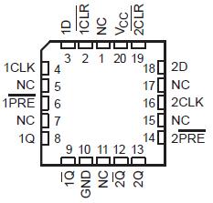 Specifications
Supply voltage range, VCC . . . . . . . . . . . . . . . . . . . . . . . . . . . . . . . . . . . . . . . 0.5 V to 7 V
Input clamp current, IIK (VI < 0 or VI > VCC) (see Note 1) . . . . . . . . . . . . . . . . . . . ±20 mA
Output clamp current, IOK (VO < 0 or VO > VCC) (see Note 1) . . . . . . . . . . . . . . . . ±20 mA
Continuous output current, IO (VO = 0 to VCC) . . . . . . . . . . . . . . . . . . . . . . . . . . . ±25 mA
Continuous current through VCC or GND . . . . . . . . . . . . . . . . . . . . . . . . . . . . . . . . . ±50 mA
Package thermal impedance, JA (see Note 2): D package . . . . . . . . . . . . . . . . . . 127°C/W
N package . . . . . . . . . . . . . . . . . . 78°C/W
PW package . . . . . . . . . . . . . . . . 170°C/W
Storage temperature range, Tstg . . . . . . . . . . . . . . . . . . . . . . . . . . . . . . . 65°C to 150°C
‡ Stresses beyond those listed under "absolute maximum ratings" may cause permanent damage to the device. These are stress ratings only, and functional operation of the device at these or any other conditions beyond those indicated under "recommended operating conditions" is not implied. Exposure to absolute-maximum-rated conditions for extended periods may affect device reliability.
NOTES: 1. The input and output voltage ratings may be exceeded if the input and output current ratings are observed.
2. The package thermal impedance is calculated in accordance with JESD 51, except for through-hole packages, which use a trace length of zero.
DescriptionThe SN54HCT74 contain two independent D-type positive-edge-triggered flip-flops. A low level at the preset (PRE) or clear (CLR) inputs sets or resets the outputs regardless of the levels of the other inputs. When PRE and CLR are inactive (high), data at the data (D) input meeting the setup time requirements are transferred to the outputs of SN54HCT74 on the positive-going edge of the clock (CLK) pulse. Clock triggering occurs at a voltage level and is not directly related to the rise time of CLK. Following the hold-time interval, data at the D input may be changed without affecting the levels at the outputs.
The SN54HCT74 is characterized for operation over the full military temperature range of 55°C to 125°C. The SN74HCT74 is characterized for operation from 40°C to 85°C.

 SN54HCT74 Data Sheet


