Features: 2-V to 5.5-V VCCOperation
Max tpdof 6.5 ns at 5 V
Typical VOLP(Output Ground Bounce)<0.8 V at VCC= 3.3 V, TA= 25°C
Typical VOHV (Output VOHUndershoot)>2.3 V at VCC= 3.3 V, TA= 25°C
Support Mixed-Mode Voltage Operation on All Ports
IoffSupports Partial-Power-Down Mode Operation
Latch-Up Performance Exceeds 250 mA Per JESD 17
ESD Protection Exceeds JESD 22
− 2000-V Human-Body Model (A114-A)
− 200-V Machine Model (A115-A)
− 1000-V Charged-Device Model (C101)
ApplicationAmplifiers amplifier.ti.com Audio
Data Converters dataconverter.ti.com Automotive
DSP dsp.ti.com Broadband
Interface interface.ti.com Digital Control
Logic logic.ti.com Military Power Mgmt power.ti.com Optical Networking
Microcontrollers microcontroller.ti.com Security
Telephony
Video & Imaging
Wireless
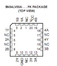
Pinout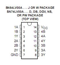
 Specifications
Supply voltage range, VCC. . . . . . . . . . . . . . . . . . . . . . . . . . . . . . . . . . . . . . .−0.5 V to 7 V
Input voltage range, VI(see Note 1) . . . . . . . . . . . . . . . . . . . . . . . . . . . . . . .−0.5 V to 7 V
Voltage range applied to any output in the high-impedance
or power-off state, VO(see Note 1). . . . . . . . . . . . . . . . . . . . . . . . . . . . . −0.5 V to 7 V
Output voltage range, VO(see Notes 1 and 2) . . . . . . . . . . . . . . . . . −0.5 V to VCC+ 0.5 V
Input clamp current, IIK(VI< 0). . . . . . . . . . . . . . . . . . . . . . . . . . . . . . . . . . . . . . . .−20 mA
Output clamp current, IOK(VO< 0). . . . . . . . . . . . . . . . . . . . . . . . . . . . . . . . . . . . . −50 mA
Continuous output current, IO (VO= 0 to VCC) . . . . . . . . . . . . . . . . . . . . . . . . . . .. ±25 mA
Continuous current through VCC or GND . . . . . . . . . . . . . . . . . . . . . . . . . . . . . . . . ±50 mA
Package thermal impedance, JA(see Note 3):D package . . . . . . . . . . . . . . . . . . . .86/W
(see Note 3):DB package . . . . . . . . . . . . . . . .. . . 96/W
(see Note 3):DGV package. . . . . . . . . . . . . . . . . 127/W
(see Note 3):NS package . . . . . . . . . . . . . . . . . . 76/W
(see Note 3):PW package . . . . . . . . . . . . . .. . . 113/W
(see Note 4):RGY package . . . . . . . . . . . . . . . . .47/W
Storage temperature range, Tstg. . . . . . . . . . . . . . . . . . . . . . . . . . . . . . . . .−65 to 150
DescriptionThese quadruple 2-input positive-NAND gates of LV00A are designed for 2-V to 5.5-V V
CCoperation.
The 'LV00A devices perform the Boolean function Y =A •B or Y = A + B in positive logic.

 SN54LV00A Data Sheet


