Features: 2-V to 5.5-V VCC Operation
Max tpd of 9 ns at 5 V
Typical VOLP (Output Ground Bounce) <0.8 V at VCC = 3.3 V, TA = 25°C
Typical VOHV (Output VOH Undershoot) >2.3 V at VCC = 3.3 V, TA = 25°C
Support Mixed-Mode Voltage Operation on All Ports
Latch-Up Performance Exceeds 250 mA Per JESD 17
ESD Protection Exceeds JESD 22
− 2000-V Human-Body Model (A114-A)
− 200-V Machine Model (A115-A)
− 1000-V Charged-Device Model (C101)Pinout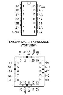 Specifications
Supply voltage range, VCC . . . . . . . . . . . . . . . . . . . . . . . . . . . . . . . . . . . . . . . . . . . . . −0.5 V to 7 V
Input voltage range, VI (see Note 1) . . . . . . . . . . . . . . . . . . . . . . . . . . . . . . . . . . . . . −0.5 V to 7 V
Output voltage range, VO (see Notes 1 and 2) . . . . . . . . . . . . . . . . . . . . . . . −0.5 V to VCC + 0.5 V
Input clamp current, IIK (VI < 0) . . . . . . . . . . . . . . . . . . . . . . . . . . . . . . . . . . . . . . . . . . . . . .−20 mA
Output clamp current, IOK (VO < 0) . . . . . . . . . . . . . . . . . . . . . . . . . . . . . . . . . . . . . . . . . . . −50 mA
Continuous output current, IO (VO = 0 to VCC) . . . . . . . . . . . . . . . . . . . . . . . . . . . . . . . . . . ±25 mA
Continuous current through VCC or GND . . . . . . . . . . . . . . . . . . . . . . . . . . . . . . . . . . . . . . . ±50 mA
Package thermal impedance, JA (see Note 3): D package . . . . . . . . . . . . . . . . . . . . . . . . . 86°C/W
DB package . . . . . . . . . . . . . . . . . . . . . . . . . 96°C/W
DGV package . . . . . . . . . . . . . . . . . . . . . . . 127°C/W
NS package . . . . . . . . . . . . . . . . . . . . . . . . . .76°C/W
PW package . . . . . . . . . . . . . . . . . . . . . . . 113°C/W
Storage temperature range, Tstg . . . . . . . . . . . . . . . . . . . . . . . . . . . . . . . . . . . . . .. −65°C to 150°C
Voltage range applied to any output in the high-impedance or power-off state, VO (see Note 1). . . . . .. −0.5 V to 7 V
Stresses beyond those listed under "absolute maximum ratings" may cause permanent damage to the device. These are stress ratings only, and functional operation of the device at these or any other conditions beyond those indicated under "recommended operating conditions" is not implied. Exposure to absolute-maximum-rated conditions for extended periods may affect device reliability.
NOTES: 1. The input and output negative-voltage ratings may be exceeded if the input and output current ratings are observed.
2. This value is limited to 5.5 V maximum.
3. The package thermal impedance is calculated in accordance with JESD 51-7.
DescriptionThe 'LV132A devices are quadruple positive-NAND gates designed for 2-V to 5.5-V V
CC operation.
The 'LV132A devices perform the Boolean function Y = A • B or Y = A + B in positive logic.
Each circuit functions of LV132A as a NAND gate, but because of the Schmitt action, it has different input threshold levels for positive- and negative-going signals.
These circuits of LV132A are temperature compensated and can be triggered from the slowest of input ramps and still give clean jitter-free output signals.

 SN54LV132A Data Sheet


