Features: 2-V to 5.5-V VCC Operation
Max tpd of 10.5 ns at 5 V
Typical VOLP (Output Ground Bounce)<0.8 V at VCC = 3.3 V, TA = 25
Typical VOHV (Output VOH Undershoot)>2.3 V at VCC = 3.3 V, TA = 25
Ioff Supports Partial-Power-Down-ModeOperation
Synchronous Load
Direct Overriding Clear
Parallel-to-Serial Conversion
Latch-Up Performance Exceeds 100 mA PerJESD 78, Class II
ESD Protection Exceeds JESD 22
− 2000-V Human-Body Model (A114-A)
− 200-V Machine Model (A115-A)
− 1000-V Charged-Device Model (C101)
Pinout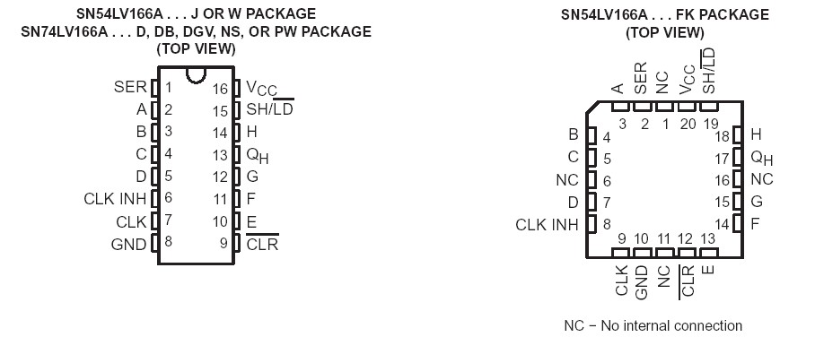 Specifications
Supply voltage range, VCC . . . . . . . . . . . . . . . . . . . . . . . . . . . . . . . . . . . . . . . . . . . . . . . . . . . . −0.5 V to 7 V
Input voltage range, VI (see Note 1) . . . . . . . . . . . . . . . . . . . . . . . . . . . . . . . . . . . . . . . . . . . .−0.5 V to 7 V
Output voltage range applied in high or low state, VO (see Notes 1 and 2) . . . . . . . .−0.5 V to VCC + 0.5 V
Voltage range applied to any output in the power-off state, VO (see Note 1) . . . . . . . . . . . . . −0.5 V to 7 V
Input clamp current, IIK (VI < 0) . . . . . . . . . . . . . . . . . . . . . . . . . . . . . . . . . . . . . . . . . . . . . . . . . . .−20 mA
Output clamp current, IOK (VO < 0) . . . . . . . . . . . . . . . . . . . . . . . . . . . . . . . . . . . . . . . . . . . . . . . . . .−50 mA
Continuous output current, IO (VO = 0 to VCC) . . . . . . . . . . . . . . . . . . . . . . . . . . . . . . . . . . . . . . . . .±25 mA
Continuous current through VCC or GND . . . . . . . . . . . . . . . . . . . . . . . . . . . . . . . . . . . . . . . . . . . . . .±50 mA
Package thermal impedance, JA (see Note 3): D package . . . . . . . . . . . . . . . . . . . . . . . . . . . . . . . . .73/W
DB package . . . . . . . . . . . . . . . . . . . . . . . . . . .. . . . . .82/W
DGV package . . . . . . . . . . . . . . . . . . . . . . . . . . . . . .120/W
NS package. . . . . . . . . . . . . . . . . . . . . . . . . . . . . . . . . 64/W
PW package . . . . . . . . . . . . . . . . . . . . . . . . . . . . . . .108/W
Storage temperature range, Tstg . . . . . . . . . . . . . . . . . . . . . . . . . . . . . . . . . . . . . . . . . . . . . . . .−65 to 150
DescriptionThe 'LV166A devices are 8-bit parallel-load shift registers, designed for 2-V to 5.5-V VCC operation.
The 'LV166A parallel-in or serial-in, serial-out registers feature gated clock (CLK, CLK INH) inputs and anoverriding clear (CLR) input. The parallel-in or serial-in modes are established by the shift/load (SH/ LD) input.When high, SH/ LD enables the serial (SER) data input and couples the eight flip-flops for serial shifting with eachclock (CLK) pulse. When low, the parallel (broadside) data inputs of LV166A are enabled, and synchronous loading occurson the next clock pulse. During parallel loading, serial data flow is inhibited. Clocking is accomplished on thelow-to-high-level edge of CLK through a 2-input positive-NOR gate, permitting one input to be used as aclock-enable or clock-inhibit function. Holding either CLK or CLK INH high inhibits clocking; holding either lowenables the other clock input. This allows the system clock to be free running, and the register can be stoppedon command with the other clock input. CLK INH should be changed to the high level only when CLK is high.CLR overrides all other inputs, including CLK, and resets all flip-flops to zero.
LV166A is fully specified for partial-power-down applications using Ioff. The Ioff circuitry disables theoutputs, preventing damaging current backflow through the devices when they are powered down.

 SN54LV166A Data Sheet


