SN54LV4052A

Features: 2-V to 5.5-V VCC OperationSupport Mixed-Mode Voltage Operation on All PortsFast SwitchingHigh On-Off Output-Voltage RatioLow Crosstalk Between SwitchesExtremely Low Input CurrentLatch-Up Performance Exceeds 100 mA Per JESD 78, Class IIESD Protection Exceeds JESD 22 − 2000-V Human-B...

product image

SN54LV4052A Picture
SeekIC No. : 004497096 Detail

SN54LV4052A: Features: 2-V to 5.5-V VCC OperationSupport Mixed-Mode Voltage Operation on All PortsFast SwitchingHigh On-Off Output-Voltage RatioLow Crosstalk Between SwitchesExtremely Low Input CurrentLatch-Up P...

floor Price/Ceiling Price

Part Number:
SN54LV4052A
Supply Ability:
5000

Price Break

  • Qty
  • 1~5000
  • Unit Price
  • Negotiable
  • Processing time
  • 15 Days
Total Cost: $ 0.00

SeekIC Buyer Protection PLUS - newly updated for 2013!

  • Escrow Protection.
  • Guaranteed refunds.
  • Secure payments.
  • Learn more >>

Month Sales

268 Transactions

Rating

evaluate  (4.8 stars)

Upload time: 2025/12/24

Payment Methods

All payment methods are secure and covered by SeekIC Buyer Protection PLUS.

Notice: When you place an order, your payment is made to SeekIC and not to your seller. SeekIC only pays the seller after confirming you have received your order. We will also never share your payment details with your seller.
Product Details

Description


Features:

 2-V to 5.5-V VCC Operation
 Support Mixed-Mode Voltage Operation on All Ports
 Fast Switching
 High On-Off Output-Voltage Ratio
 Low Crosstalk Between Switches
 Extremely Low Input Current
 Latch-Up Performance Exceeds 100 mA Per JESD 78, Class II
 ESD Protection Exceeds JESD 22
   − 2000-V Human-Body Model (A114-A)
   − 200-V Machine Model (A115-A)
   − 1000-V Charged-Device Model (C101)


Application

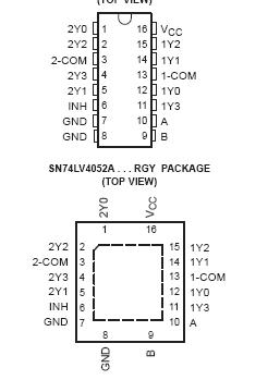
  Connection Diagram


Specifications

Supply voltage range, VCC . . . . . . . . . . . . . . . . . . . . . . . . . . . . . . . . . . . . . . . . . . . . . . . . . . . . . . −0.5 V to 7.0 V
Input voltage range, VI (see Note 1) . . . . . . . . . . . . . . . . . . . . . . . . . . . . . . . . . . . . . . . . . . . . . . −0.5 V to 7.0 V
Switch I/O voltage range, VIO (see Notes 1 and 2) . . . . . . . . . . . . . . . . . . . . . . . . . . . . . . −0.5 V to VCC + 0.5 V
Input clamp current, IIK (VI < 0) . . . . . . . . . . . . . . . . . . . . . . . . . . . . . . . . . . . . . . . . . . . . . . . . . . . . . . . . −20 mA
I/O diode current, IIOK (VIO < 0) . . . . . . . . . . . . . . . . . . . . . . . . . . . . . . . . . . . . . . . . . . . . . . . . . . . . . . .. −50 mA
Switch through current, IT (VIO = 0 to VCC) . . . . . . . . . . . . . . . . . . . . . . . . . . . . . . . . . . . . . . . . . . . . . . . ±25 mA
Continuous current through VCC or GND . . . . . . . . . . . . . . . . . . . . . . . . . . . . . . . . . . . . . . . . . . . . . . . . .. ±50 mA
Package thermal impedance, JA (see Note 3): D package . . . . . . . . . . . . . . . . . . . . . . . . . . . . . . . . .  . 73°C/W
                                                     (see Note 3): DB package . . . . . . . . . . . . . . . . . . . . . . . . . . . . . . . . . 82°C/W
                                                     (see Note 3): DGV package . . . . . . . . . . . . . . . . . . . . . . . . . . . . . . . 120°C/W
                                                     (see Note 3): N package . . . . . . . . . . . . . . . . . . . . . . . . . . . . . . . . . . 67°C/W
                                                     (see Note 3): NS package . . . . . . . . . . . . . . . . . . . . . . . . . . . . . . . . . 64°C/W
                                                     (see Note 3): PW package . . . . . . . . . . . . . . . . . . . . . . . . . . . . . . .  108°C/W
                                                     (see Note 4): RGY package . . . . . . . . . . . . . . . . . . . . . . . . . . . . . . . . 39°C/W
Storage temperature range, Tstg . . . . . . . . . . . . . . . . . . . . . . . . . . . . . . . . . . . . . . . . . . . . . .  −65°C to 150°C
NOTES: 1. The input and output negative-voltage ratings may be exceeded if the input and output current ratings are observed.
             2. This value is limited to 5.5 V maximum.
             3. The package thermal impedance is calculated in accordance with JESD 51-7.
             4. The package thermal impedance is calculated in accordance with JESD 51-5.


Description

These dual 4-channel CMOS analog multiplexers/demultiplexers are designed for 2-V to 5.5-V VCC operation.

The 'LV4052A devices handle both analog and digital signals. Each channel permits signals with amplitudes up to 5.5 V (peak) to be transmitted in either direction.

LV4052A applications include signal gating, chopping, modulation or demodulation (modem), and signal multiplexing for analog-to-digital and digital-toanalog conversion systems.


Customers Who Bought This Item Also Bought

Margin,quality,low-cost products with low minimum orders. Secure your online payments with SeekIC Buyer Protection.
Static Control, ESD, Clean Room Products
Cables, Wires - Management
Soldering, Desoldering, Rework Products
Programmers, Development Systems
Audio Products
Transformers
View more