Features: EPICTM (Enhanced-Performance ImplantedCMOS) Submicron Process
ESD Protection Exceeds 2000 V Per MIL-STD-883, Method 3015; Exceeds 200 V Using Machine Model (C = 200 pF, R = 0)
Latch-Up Performance Exceeds 250 mA Per JESD 17
Typical VOLP (Output Ground Bounce)< 0.8 V at VCC = 3.3 V, TA = 25
Typical VOHV (Output VOH Undershoot)> 2 V at VCC = 3.3 V, TA = 25
Inputs Accept Voltages to 5.5 V
Package Options Include Plastic Small-Outline (D), Shrink Small-Outline (DB), and Thin Shrink Small-Outline (PW) Packages, Ceramic Chip Carriers (FK), Ceramic Flat (W) Package, and DIPs (J)
Pinout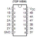 Specifications
Supply voltage range, VCC . . . . . . . . . . . . . . . . . . . . . . . . . . . . . . . . . . . . . . . .. . . . . . . . 0.5 V to 6.5 V
Input voltage range, VI (see Note 1) . . . . . . . . . . . . . . . . . . . . . . . . . . . . . . . . . . . . . . . . 0.5 V to 6.5 V
Output voltage range, VO (see Notes 1 and 2) . . . . . . . . . . . . . . . . .. . . . . . . . . . . 0.5 V to VCC + 0.5 V
Input clamp current, IIK (V I< 0) . . . . . . . . . . . . . . . . . . . . . . . . . . . . . . . . . . . . . . . .. . . . . . . . . . 50 mA
Output clamp current, IOK (VO < 0) . . . . . . . . . . . . . . . . . . . . . . . . . . . . . . . . . . . . . . . . . . . . . . . . 50 mA
Continuous output current, IO . . . . . . . . . . . . . . . . . . . . . . . . . . . . . . . . . . . . . . . . . . . . . . . . . . . ±50 mA
Continuous current through VCC or GND . . . . . . . . . . . . . . . . . . . . . . . . . . . . . . . . .. . . . . . . . . . ±100 mA
Package thermal impedance, JA (see Note 3): D package . . . .. . . . . . . . .. . . . . . . . . . . . . . . . . 127°C/W
DB package . . . . . . . . . . . . . . . . . . . . . . . . . . . . 158°C/W
PW package . . . . . . . . . . . . . . . . . . . . . . . . . . . . 170°C/W
Storage temperature range, Tstg . . . . . . . . . . . . . . . . . . . . . . . . . . . . . . . . . . . . . . . . . . . . 65°Cto 150°C
DescriptionThe SN54LVC00A quadruple 2-input positive-NAND gate is designed for 2.7-V to 3.6-V VCCoperation and the SN74LVC00A quadruple 2-input positive-NAND gate is designed for 1.65-Vto 3.6-V VCC operation.
The SN54LVC00A devices perform the Boolean function Y = A • B or Y = A + B in positive logic.
Inputs of SN54LVC00A can be driven from either 3.3-V or 5-V devices. This feature allows the use of these devices as translators in a mixed 3.3-V/5-V system environment.
The SN54LVC00A is characterized for operation over the full military temperature range of 55°C to 125°C. The SN74LVC00A is characterized for operation from 40°C to 85°C.

 SN54LVC00A Data Sheet


