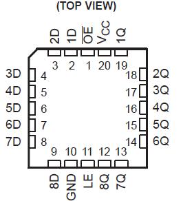
Pinout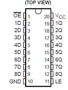
 Specifications
Supply voltage range, VCC . . . . . . . . . . . . . . . . . . . . . . . . . . . . . . . 0.5 V to 6.5 V
Input voltage range, VI (see Note 1) . . . . . . . . . . . . . . . . . . . . . . . .0.5 V to 6.5 V
Voltage range applied to any output in the high-impedance or power-off state, VO
(see Note 1) . . . . . . . . . . . . . . . . . . . . . . . . . . . . . . . . . . . . . . . ......0.5 V to 6.5 V
Voltage range applied to any output in the high or low state, VO
(see Notes 1 and 2) . . . . . . . . . . . . . . . . . . . . . . . . . . . . . . .0.5 V to VCC + 0.5 V
Input clamp current, IIK (VI < 0) . . . . . . . . . . . . . . . . . . . . . . . . . . . . . . . . 50 mA
Output clamp current, IOK (VO < 0) . . . . . . . . . . . . . . . . . . . . . . . . . . . . . .50 mA
Continuous output current, IO . . . . . . . . . . . . . . . . . . . . . . . . . . . . . . . . . .±50 mA
Continuous current through VCC or GND . . . . . . . . . . . . . . . . . . . . . . . . .±100 mA
Package thermal impedance, qJA (see Note 3): DB package . . . . . . . . . .115°C/W
DW package . . . . . . . . . . 97°C/W
PW package . . . . . . . . . .128°C/W
Storage temperature range, Tstg . . . . . . . . . . . . . . . . . . . . . . . .65°C to 150°C
DescriptionThe SN54LVC573A octal transparent D-type latch is designed for 2.7-V to 3.6-V VCC operation and the SN74LVC573A octal transparent D-type latch is designed for 1.65-V to 3.6-V VCC operation.
SN54LVC573A feature 3-state outputs designed specifically for driving highly capacitive or relatively low-impedance loads. SN54LVC573A is particularly suitable for implementing buffer registers, input/output (I/O) ports, bidirectional bus drivers, and working registers.
While the latch-enable (LE) input is high, the Q outputs follow the data (D) inputs. When LE is taken low, the Q outputs are latched at the logic levels at the D inputs.
A buffered output-enable (OE) input of SN54LVC573A can be used to place the eight outputs in either a normal logic state (high or low logic levels) or a high-impedance state. In the high-impedance state, the outputs of SN54LVC573A neither load nor drive the bus lines significantly. The high-impedance state and increased drive provide the capability to drive bus lines without interface or pullup components.
OE does not affect the internal operations of the latches. Old data of SN54LVC573A can be retained or new data can be entered while the outputs are in the high-impedance state.
To ensure the high-impedance state during power up or power down, OE should be tied to VCC through a pullup resistor; the minimum value of the resistor SN54LVC573A is determined by the current-sinking capability of the driver.
Inputs of SN54LVC573A can be driven from either 3.3-V or 5-V devices. This feature allows the use of these devices as translators in a mixed 3.3-V/5-V system environment.

 SN54LVC573A Data Sheet


