Features: EPICETM (Enhanced-Performance Implanted CMOS) Submicron Process
Typical VOLP (Output Ground Bounce) < 0.8 V at VCC = 3.3 V, TA = 25°C
Typical VOHV (Output VOH Undershoot)> 2 V at VCC = 3.3 V, TA = 25°C
Support Mixed-Mode Signal Operation on All Ports (5-V Input/Output Voltage With 3.3-V VCC)
ESD Protection Exceeds 2000 V Per MIL-STD-883, Method 3015; Exceeds 200 V Using Machine Model (C = 200 pF, R = 0)
Package Options Include Plastic Small-Outline (DW), Shrink Small-Outline (DB), Thin Shrink Small-Outline (PW) Packages, and Ceramic Chip Carriers (FK)Pinout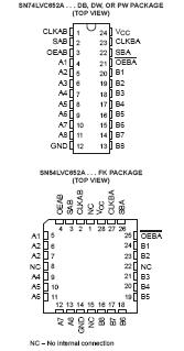 SpecificationsSupply voltage range, VCC . . . . . . . . . . . . . . . . . . . . . . . . . . . . . . . . . . . . . . . . . . . . . . . . . . .. . . 0.5 V to 6.5 V
Input voltage range, VI (see Note 1) . . . . . . . . . . . . . . . . . . . . . . . . . . . . . . . . . . . . . . . . . . . . . . 0.5 V to 6.5 V
Voltage range applied to any output in the high-impedance or power-off state, VO
(see Note 1) . . . . . . . . . . . . . . . . . . . . . . . . . . . . . . . . . . . . . . . . . . . . . . . . . . . . . . . . . . . . . . . . . 0.5 V to 6.5 V
Voltage range applied to any output in the high or low state, VO
(see Notes 1 and 2) . . . . . . . . . . . . . . . . . . . . . . . . . . . . . . . . . . . . . . . . . . . . . . . . . . . . . . 0.5 V to VCC + 0.5 V
Input clamp current, IIK (VI < 0) . . . . . . . . . . . . . . . . . . . . . . . . . . . . . . . . . . . . . . . . . . . . . . . . . . . . . . . . 50 mA
Output clamp current, IOK (VO < 0) . . . . . . . . . . . . . . . . . . . . . . . . . . . . . . . . . . . . . . . . . . . . . . . . . . . . .. 50 mA
Continuous output current, IO . . . . . . . . . . . . . . . . . . . . . . . . . . . . . . . . . . . . . . . . . . . . . . . . . . . . . . . . .. ±50 mA
Continuous current through VCC or GND . . . . . . . . . . . . . . . . . . . . . . . . . . . . . . . . . . . . . . . . . . . . . . .. . ±100 mA
Package thermal impedance, qJA (see Note 3): DB package . . . . . . . . . . . . . . . . . . . . . . . . . . . . . . . .... 104°C/W
DW package . . . . . . . . . . . . . . . . . . . . . . . . . . . . . . . . .... 81°C/W
PW package . . . . . . . . . . . . . . . . . . . . . . . . . . . . . . . .... 120°C/W
Storage temperature range, Tstg . . . . . . . . . . . . . . . . . . . . . . . . . . . . . . . . . . . . . . . . . . . . . . . .. 65°C to 150°C
NOTES: 1. The input negative-voltage and output voltage ratings may be exceeded if the input and output current ratings are observed.
2. The value of VCC is provided in the recommended operating conditions table.
3. The package thermal impedance is calculated in accordance with JESD 51.DescriptionThe SN54LVC652A octal bus transceiver and register is designed for 2.7-V to 3.6-V VCC operation, and the SN74LVC652A octal bus transceiver and register is designed for 1.65-V to 3.6-V VCC operation.
SN54LVC652A consists of bus transceiver circuits, D-type flip-flops, and control circuitry arranged for multiplexed transmission of data directly from the data bus or from the internal storage registers.
Output-enable (OEAB and OEBA) inputs of SN54LVC652A are provided to control the transceiver functions.Select-control (SAB and SBA) inputs are provided to select whether real-time or stored data is transferred. The circuitry used for select control eliminates the typical decoding glitch that occurs in a multiplexer during the transition between stored and real-time data. A low input selects real-time data, and a high input selects stored data. Figure 1 illustrates the four fundamental bus-management functions that are performed with the SN54LVC652A.
Data on the A or B data bus, or both, SN54LVC652A is stored in the internal D-type flip-flops by low-to-high transitions at the appropriate clock (CLKAB or CLKBA) inputs, regardless of the select- or enable-control pins. When SAB and SBA are in the real-time transfer mode, SN54LVC652A is possible to store data without using the internal D-type flip-flops by simultaneously enabling OEAB and OEBA. In this configuration, each output reinforces its input. When all other data sources to the two sets of bus lines are at high impedance, each set of bus lines remains at its last state.
Inputs of SN54LVC652A can be driven from either 3.3-V or 5-V devices. This feature allows the use of these devices as translators in a mixed 3.3-V/5-V system environment.

 SN54LVC652A Data Sheet


