Features: ·State-of-the-Art Advanced BiCMOS Technology (ABT) Design for 3.3-V Operation and Low-Static Power Dissipation
·Members of the Texas Instruments WidebusE Family
·Support Mixed-Mode Signal Operation (5-V Input and Output Voltages With 3.3-V VCC)
·Support Unregulated Battery Operation Down to 2.7 V
·Typical VOLP (Output Ground Bounce) < 0.8 V at
VCC = 3.3 V, T
A = 25°C
·ESD Protection Exceeds 2000 V Per MIL-STD-883C, Method 3015; Exceeds 200 V Using Machine Model (C = 200 pF, R = 0)
· Latch-Up Performance Exceeds 500 mA Per JEDEC Standard JESD-17
·Bus-Hold Data Inputs Eliminate the Need for External Pullup Resistors
·Support Live Insertion
·Distributed VCC and GND Pin Configuration Minimizes High-Speed Switching Noise
· Flow-Through Architecture Optimizes PCB Layout
· Package Options Include Plastic 300-mil
Shrink Small-Outline (DL) and Thin Shrink
Small-Outline (DGG) Packages and 380-mil
Fine-Pitch Ceramic Flat (WD) Package
Using 25-mil Center-to-Center Spacings Pinout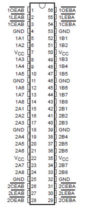 Specifications
Supply voltage range, VCC . . . . . . . . . . . . . . . . . . . . . . . . . . . . . . . . . . . . . . . . . . . . . . . . 0.5 V to 4.6 V
Input voltage range, VI (see Note 1) . . . . . . . . . . . . . . . . . . . . . . . . . . . . . . . . . . . . . . . . . . .0.5 V to 7 V
Voltage range applied to any output in the high state or power-off state, VO (see Note 1). .0.5 V to 7 V
Current into any output in the low state, IO: SN54LVT16543 . . . . . . . . . . . . . . . . . . . . . . . . . . . . . . 96 mA
SN74LVT16543 . . . . . . . . . . . . . . . . . . . . . . . . . . . . . 128 mA
Current into any output in the high state, IO (see Note 2): SN54LVT16543 . . . . . . . . . . . . . .. . . . . . 48 mA
SN74LVT16543 . . . . . . . . . . . . . . . . . . . . 64 mA
Input clamp current, IIK (VI < 0) . . . . . . . . . . . . . . . . . . . . . . . . . . . . . . . . . . . . . . . . . . . . . . . . . . . . 50 mA
Output clamp current, IOK (VO < 0) .. . . . . . . . . . . . . . . . . . . . . . . . . . . . . . . . . . . . . . . . . . . . . . . . . 50 mA
Maximum power dissipation at TA = 55°C (in still air) (see Note 3): DGG package . . . . . . . . . . . . . . . . . 1 W
DL package . . . . . . . . . . . . . . . . . 1.4 W
Storage temperature range, Tstg . . . . . . . . . . . . . . . . . . . . . . . . . . . . . . . . . . . . . . . . . . . . 65°C to 150°C
§ Stresses beyond those listed under "absolute maximum ratings" may cause permanent damage to the device. These are stress ratings only, and functional operation of the device at these or any other conditions beyond those indicated under "recommended operating conditions" is not implied. Exposure to absolute-maximum-rated conditions for extended periods may affect device reliability.
NOTES: 1. The input and output negative-voltage ratings may be exceeded if the input and output clamp-current ratings are observed.
2. This current flows only when the output is in the high state and VO > VCC.
3. The maximum package power dissipation is calculated using a junction temperature of 150°C and a board trace length of 750 mils.
For more information, refer to the Package Thermal Considerations application note in the 1994 ABT Advanced BiCMOS Technology Data Book, literature number SCBD002B.
DescriptionThe 'LVT16543 are 16-bit registered transceivers designed for low-voltage (3.3-V) VCC operation, but with the capability to provide a TTL interface to a 5-V system environment. These devices can be used as two 8-bit transceivers or one 16-bit transceiver. Separate latch-enable (LEAB or LEBA) and output-enable (OEAB or OEBA) inputs of LVT16543 are provided for each register to permit independent control in either direction of data flow.
The A-to-B enable (CEAB) input of LVT16543 must be low in order to enter data from A or to output data from B. If LEAB is low and LEAB is low, the A-to-B latches are transparent; a subsequent low-to-high transition of LEAB puts the A latches in the storage mode. With CEAB and OEAB both low, the 3-state B outputs of LVT16543 are active and reflect the data present at the output of the A latches. Data flow from B to A is similar but requires using the CEBA,LEBA, and OEBA inputs.

 SN54LVT16543 Data Sheet


