SN54LVT182512

ApplicationAudiowww.ti.com/audioAutomotive www.ti.com/automotiveBroadband www.ti.com/broadbandDigital Control www.ti.com/digitalcontrolMilitary www.ti.com/militaryOptical Networking www.ti.com/opticalnetworkSecurity www.ti.com/securityTelephony www.ti.com/telephonyVideo & Imaging www.ti.com/vi...

product image

SN54LVT182512 Picture
SeekIC No. : 004497156 Detail

SN54LVT182512: ApplicationAudiowww.ti.com/audioAutomotive www.ti.com/automotiveBroadband www.ti.com/broadbandDigital Control www.ti.com/digitalcontrolMilitary www.ti.com/militaryOptical Networking www.ti.com/optic...

floor Price/Ceiling Price

Part Number:
SN54LVT182512
Supply Ability:
5000

Price Break

  • Qty
  • 1~5000
  • Unit Price
  • Negotiable
  • Processing time
  • 15 Days
Total Cost: $ 0.00

SeekIC Buyer Protection PLUS - newly updated for 2013!

  • Escrow Protection.
  • Guaranteed refunds.
  • Secure payments.
  • Learn more >>

Month Sales

268 Transactions

Rating

evaluate  (4.8 stars)

Upload time: 2025/12/24

Payment Methods

All payment methods are secure and covered by SeekIC Buyer Protection PLUS.

Notice: When you place an order, your payment is made to SeekIC and not to your seller. SeekIC only pays the seller after confirming you have received your order. We will also never share your payment details with your seller.
Product Details

Description


Application

Audio                                www.ti.com/audio
Automotive                       www.ti.com/automotive
Broadband                        www.ti.com/broadband
Digital Control                   www.ti.com/digitalcontrol
Military                              www.ti.com/military
Optical Networking           www.ti.com/opticalnetwork
Security                            www.ti.com/security
Telephony                        www.ti.com/telephony
Video & Imaging               www.ti.com/video
Wireless                           www.ti.com/wireless


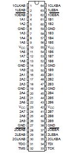
Pinout

  Connection Diagram


Specifications

Supply voltage range, VCC . . . . . . . . . . . . . . .  . . . . . . . 0.5 V to 4.6 V
Input voltage range, VI (see Note 1)  . . . . . . . . . . .. . . . . 0.5 V to 7 V
Voltage range applied to any output in the high or power-off state,
VO (see Note 1).  . . . . . . . . . . . . .  . . . . . . . . . . . . .  . . . . .0.5 V to 7 V
Current into any output in the low state,
IO: SN54LVT18512. . . . . . . . . . .  . . . . . . . . . ..  . . . . . . . . . . . .  . . 96 mA
      SN54LVT182512 (A port or TDO).  . . . . . . ..  . . . . . . . . .. . .  . . 96 mA
      SN54LVT182512 (B port)  . . . . . . . . . . . . ..  . . . . . . . .  . . .  .. . 30 mA
      SN74LVT18512 . . . . . . . . . . . . . .  . . . . . .  . . . . . . . . . . . . . .  128 mA
      SN74LVT182512 (A port or TDO). . . . . . . . . .  . . . . . . . . . . . . 128 mA
      SN74LVT182512 (B port) . . . . . . . .. . . . . . . .  . . . . . . . . . . . . . .30 mA
Current into any output in the high state,
IO (see Note 2): SN54LVT18512. . . . . . . . .  . . . . .  . . . . . . . . . . . . 48 mA
                           SN54LVT182512 (A port or TDO) . .  . . . . .. . . . . . 48 mA
                           SN54LVT182512 (B port)  . . . .. . ..  . . .  . . . . . . .  30 mA
                           SN74LVT18512 . . . . . . . . . . . . ..  . . . . . . . .  . . . . 64 mA
                           SN74LVT182512 (A port or TDO)  .  . . . .. . . . .  . . 64 mA
                           SN74LVT182512 (B port) . . .. . . . .  . . .. . . . . .  . . 30 mA
Input clamp current, IIK (VI < 0) . .  . . . . . . . . . . . . . . . . .  . . .    . 50 mA
Output clamp current, IOK (VO < 0)  . . . . . . .  . . . . . . . . .  . . .. .. . 50 mA
Package thermal impedance, JA (see Note 3): DGG package. . . 73°C/W
Storage temperature range, Tstg . . . . . . . . . . . . . . . . . . 65°C to 150°C
† Stresses beyond those listed under "absolute maximum ratings" may cause permanent damage to the device. These are stress ratings only, and functional operation of the device at these or any other conditions beyond those indicated under "recommended operating conditions" is not implied. Exposure to absolute-maximum-rated conditions for extended periods may affect device reliability.
NOTES: 1. The input and output negative-voltage ratings can be exceeded if the input and output clamp-current ratings are observed.
             2. This current only flows when the output is in the high state and VO > VCC.
             3. The package thermal impedance is calculated in accordance with JESD51.


Description

The 'LVT18512 and 'LVT182512 scan test devices with 18-bit universal bus transceivers are members of the Texas Instruments SCOPEETM testability integrated-circuit family. 'LVT18512 and 'LVT182512 supports IEEE Std 1149.1-1990 boundary scan to facilitate testing of complex circuit-board assemblies. Scan access to the test circuitry is accomplished via the 4-wire test access port (TAP) interface.

Additionally, 'LVT18512 and 'LVT182512 are designed specifically for low-voltage (3.3-V) VCC operation, but with the capability to provide a TTL interface to a 5-V system environment.


Customers Who Bought This Item Also Bought

Margin,quality,low-cost products with low minimum orders. Secure your online payments with SeekIC Buyer Protection.
Integrated Circuits (ICs)
Soldering, Desoldering, Rework Products
Semiconductor Modules
Tapes, Adhesives
803
Line Protection, Backups
View more