Features: ` State-of-the-Art Advanced BiCMOS Technology (ABT) Design for 3.3-V Operation and Low Static-Power Dissipation
` Support Mixed-Mode Signal Operation (5-V Input and Output Voltages With 3.3-V VCC)
` Support Unregulated Battery Operation Down to 2.7 V
` Typical VOLP (Output Ground Bounce) <0.8 V at VCC = 3.3 V, TA = 25°C
` Ioff and Power-Up 3-State Support Hot Insertion
` Latch-Up Performance Exceeds 100 mA Per JESD 78, Class II
` ESD Protection Exceeds JESD 22
2000-V Human-Body Model (A114-A)
200-V Machine Model (A115-A)
1000-V Charged-Device Model (C101)
` Package Options Include Plastic Small-Outline (DW), Shrink Small-Outline (DB), and Thin Shrink Small-Outline (PW)
Packages, Ceramic Chip Carriers (FK), Ceramic Flat (W) Packages, and Ceramic (J) DIPs
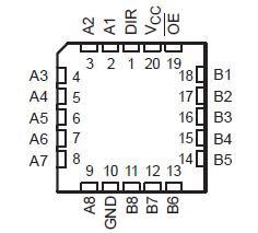
Pinout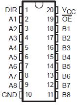
 Specifications
Supply voltage range, VCC . . . . . . . . . . . . . . . . . . . . . . . . . . . . . . . . . . . . . . . . . . . 0.5 V to 4.6 V
Input voltage range, VI (see Note 1) . . . . . . . . . . . . . . . . . . . . . . . . . . . . . . . . . . . . 0.5 V to 7 V
Voltage range applied to any output in the high-impedance
or power-off state, VO (see Note 1) . . . . . . . . . . . . . . . . . . . . . . . . . . . . . . . . . . . . . 0.5 V to 7 V
Voltage range applied to any output in the high state, VO (see Note 1) . . 0.5 V to VCC + 0.5 V
Current into any output in the low state, IO: SN54LVT245B . . . . . . . . . . . . . . . . . . . . . . . . 96 mA
SN74LVT245B . . . . . . . . . . . . . . . . . . . . . . . 128 mA
Current into any output in the high state, IO (see Note 2): SN54LVT245B . . . . . . . . . . . . . 48 mA
SN74LVT245B . . . . . . . . . . . . . 64 mA
Input clamp current, IIK (VI < 0) . . . . . . . . . . . . . . . . . . . . . . . . . . . . . . .. . . . . . . . . . . . . . 50 mA
Output clamp current, IOK (VO < 0) . . . . . . . . . . . . . . . . . . . . . . . . . . . . . . . . . . . . . . . . . .. 50 mA
Package thermal impedance, qJA (see Note 3): DB package . . . . . . . . . . . . . . . . . . . . . . . 70°C/W
DW package . . . . . . . . . . . . . . . . . . . . . . 58°C/W
PW package . . . . . . . . . . . . . . . . . . . .. . . 83°C/W
Storage temperature range, Tstg . . . . . . . . . . . . . . . . . . . . . . . . . . . . . . . . . . . . 65°C to 150°C
† Stresses beyond those listed under "absolute maximum ratings" may cause permanent damage to the device. These are stress ratings only, and functional operation of the device at these or any other conditions beyond those indicated under "recommended operating conditions" is not implied. Exposure to absolute-maximum-rated conditions for extended periods may affect device reliability.
NOTES: 1. The input and output negative-voltage ratings may be exceeded if the input and output clamp-current ratings are observed.
2. This current flows only when the output is in the high state and VO > VCC.
3. The package thermal impedance is calculated in accordance with JESD 51.
DescriptionThese octal bus transceivers are designed specifically for low-voltage (3.3-V) VCC operation, but with the capability to provide a TTL interface to a 5-V system environment.
SN54LVT245B is designed for asynchronous communication between data buses. They transmit data from the A bus to the B bus or from the B bus to the A bus, depending on the logic level at the direction-control (DIR) input. The output-enable (OE) input of SN54LVT245B can be used to disable the devices so the buses are effectively isolated.
When VCC is between 0 and 1.5 V, the SN54LVT245B is in the high-impedance state during power up or power down. However, to ensure the high-impedance state above 1.5 V, OE should be tied to VCC through a pullup resistor; the minimum value of the resistor SN54LVT245B is determined by the current-sinking capability of the driver.
SN54LVT245B is fully specified for hot-insertion applications using Ioff and power-up 3-state. The Ioff circuitry disables the outputs, preventing damaging current backflow through the devices when they are powered down.
The power-up 3-state circuitry of SN54LVT245B places the outputs in the high-impedance state during power up and power down,
which prevents driver conflict.
The SN54LVT245B is characterized for operation over the full military temperature range of 55°C to 125°C. The SN74LVT245B is characterized for operation from 40°C to 85°C.

 SN54LVT245B Data Sheet


