Features: · Members of the Texas Instruments WidebusTM Family
· State-of-the-Art Advanced BiCMOS Technology (ABT) Design for 3.3-V Operation and Low Static-Power Dissipation
· Output Ports Have Equivalent 22-W Series Resistors, So No External Resistors Are Required
· Support Mixed-Mode Signal Operation (5-V Input and Output Voltages With 3.3-V VCC)
· Support Unregulated Battery Operation Down to 2.7 V
· Typical VOLP (Output Ground Bounce) < 0.8 V at VCC = 3.3 V, TA = 25°C
· Ioff and Power-Up 3-State Support Hot Insertion
· Bus Hold on Data Inputs Eliminates the Need for External Pullup/Pulldown Resistors
· Distributed VCC and GND Pin Configuration Minimizes High-Speed Switching Noise
· Flow-Through Architecture Optimizes PCB Layout
· Latch-Up Performance Exceeds 500 mA Per JESD 17
· ESD Protection Exceeds 2000 V Per MIL-STD-883, Method 3015; Exceeds 200 V Using Machine Model (C = 200 pF, R = 0)
· Package Options Include Plastic Shrink Small-Outline (DL) and Thin Shrink Small-Outline (DGG) Packages and 380-mil Fine-Pitch Ceramic Flat (WD) Package Using 25-mil Center-to-Center Spacings
Pinout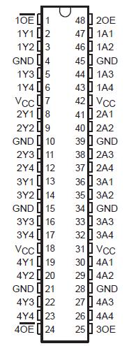 Specifications
Supply voltage range, VCC . . . . . . . . . . . . . . . . . . . . . . . . . . . . . . . . . . . . . . . . .. . . . . 0.5 V to 4.6 V
Input voltage range, VI (see Note 1) . . . . . . . . . . . . . . . . . . . . . . . . . . . . . . . . . . . . . . . 0.5 V to 7 V
Voltage range applied to any output in the high-impedance
or power-off state, VO (see Note 1) . . . . . . . . . . . . . . . . . . . . . . . . . . . . . . . . . . . . . . 0.5 V to 7 V
Voltage range applied to any output in the high state, VO (see Note 1) . . . .. . 0.5 V to VCC + 0.5 V
Current into any output in the low state, IO . . . . . . . . . . . . . . . . . . . . . . . . . . . . . . . . . . . .. . . . 30 mA
Current into any output in the high state, IO (see Note 2) . . . . . . . . . . . . . . . . . . . . . . . . . . .. . 30 mA
Input clamp current, IIK (VI < 0) . . . . . . . . . . . . . . . . . . . . . . . . . . . . . . . . . . . . . . . . . . . . . . . 50 mA
Output clamp current, IOK (VO < 0) . . . . . . . . . . . . . . . . . . . . . . . . . . . . . . . . . . . . . . . . . . .. . . 50 mA
Package thermal impedance, JA (see Note 3): DGG package . . . . . . . . . . . . . . . . . . . . . . . . . 89°C/W
DL package . . . . . . . . . . . . . . . . . . . . . . . . . . 94°C/W
Storage temperature range, Tstg . . . . . . . . . . . . . . . . . . . . . . . . . . . . . . . . . . . . . . . 65°C to 150°C
† Stresses beyond those listed under "absolute maximum ratings" may cause permanent damage to the device. These are stress ratings only, and functional operation of the device at these or any other conditions beyond those indicated under "recommended operating conditions" is not implied. Exposure to absolute-maximum-rated conditions for extended periods may affect device reliability.
NOTES: 1. The input and output negative-voltage ratings may be exceeded if the input and output clamp-current ratings are observed.
2. This current flows only when the output is in the high state and VO > VCC.
3. The package thermal impedance is calculated in accordance with JESD 51.
DescriptionThese 16-bit buffers/drivers of SN54LVTH162241 are designed specifically for low-voltage (3.3-V) VCC operation, but with the capability to provide a TTL interface to a 5-V system environment.
The devices can be used as four 4-bit buffers, two 8-bit buffers, or one 16-bit buffer. The SN54LVTH162241 provide noninverting outputs and complementary output-enable (OE and OE) inputs.
The outputs, SN54LVTH162241 is designed to source or sink up to 12 mA, include equivalent 22-W series resistors to reduce overshoot and undershoot.

 SN54LVTH162241 Data Sheet


