ApplicationAudio
Automotive
Broadband
Digital Control
Military
Optical Networking
Security
Telephony
Video & Imaging
WirelessPinout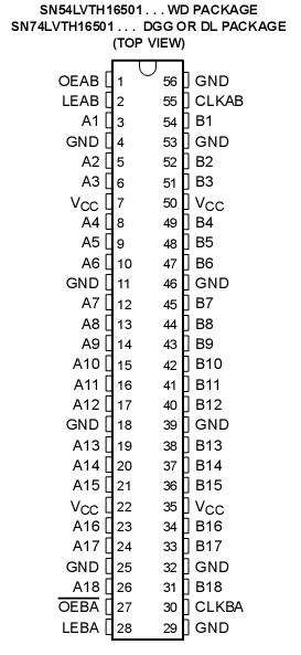 Specifications
Supply voltage range, V CC . . . . . . . . . . . . . . . . . . . . . . . . . . . . . . . . . . . . . . . . . . . . . . . . 0.5 V to 4.6 V
Input voltage range, VI (see Note 1) . . . . . . . . . . . . . . . . . . . . . . . . . . . . . . . . . . . . . . . . . . 0.5 V to 7 V
Voltage range applied to any output in the high-impedance
or power-off state, VO (see Note 1) . . . . . . . . . . . . . . . . . . . . . . . . . . . . . . . . . . . . . . . . ... .. 0.5 V to 7 V
Voltage range applied to any output in the high state, VO (see Note 1) . . . . . . . . 0.5 V to V CC + 0.5 V
Current into any output in the low state, IO : SN54LVTH16501. . . . . . . . . . . . . . . . . . . . . . . . ....... . 96 mA
SN74LVTH16501 . . . . . . . . . . . . . . . . . . . . . . . . . ..... 128 mA
Current into any output in the high state, IO (see Note 2): SN54LVTH16501 . . . . . . . . . . . . . . . . . . 48 mA
SN74LVTH16501 . . . . . . . . . . . . . .. . .... ..64 mA
Input clamp current, IIK (VI < 0) . . . . . . . . . . . . . . . . . . . . . . . . . . . . . . . . . . . . . . . . . . . . . . . . . . . 50 mA
Output clamp current, IOK (V O < 0) . . . . . . . . . . . . . . . . . . . . . . . . . . . . . . . . . . . . . . . . . . . . . . . . . 50 mA
Package thermal impedance, JA (see Note 3): DGG package . . . . . . . . . . . . . . . . . . . . . . . . . .......... 64/W
DL package . . . . . . . . . . . . . . . . . . . . . . . . . . ........... 56/W
Storage temperature range, Tstg . . . . . . . . . . . . . . . . . . . . . . . . . . . . . . . . . . . . . . . . . . . . ... 65 to 150
DescriptionThe 'LVTH16501 devices are 18-bit universal bus transceivers designed for low-voltage (3.3-V) VCCoperation, but with the capability to provide a TTL interface to a 5-V system environment.
Data flow in each direction is controlled by output-enable (OEAB and OEBA) , latch-enable (LEAB and LEBA), and clock (CLKAB and CLKBA) inputs. For A-to-B data flow, the LVTH16501 operate in the transparent mode when LEAB is high. When LEAB is low, the A data is latched if CLKAB is held at a high or low logic level. If LEAB is low, the A data is stored in the latch/flip-flop on the low-to-high transition of CLKAB. When OEAB is high, the outputs of LVTH16501 are active. When OEAB is low, the outputs are in the high-impedance state.
Data flow for B to A is similar to that of A to B but usesOEBA, LEBA, and CLKBA. The output of LVTH16501 enables are complementary (OEAB is active high and OEBA is active low).
Active bus-hold circuitry of LVTH16501 holds unused or undriven inputs at a valid logic state. Use of pullup or pulldown resistors with the bus-hold circuitry is not recommended.
When VCC is between 0 and 1.5 V, the LVTH16501 is in the high-impedance state during power up or power down. However, to ensure the high-impedance state above 1.5 V, OE should be tied to VCC through a pullup resistor and OE should be tied to GND through a pulldown resistor; the minimum value of the resistor LVTH16501 is determined by the current-sinking/current-sourcing capability of the driver.
LVTH16501 is fully specified for hot-insertion applications using Ioff and power-up 3-state. The Ioff circuitry disables the outputs, preventing damaging current backflow through the devices when they are powered down The power-up 3-state circuitry of LVTH16501 places the outputs in the high-impedance state during power up and power down which prevents driver conflict.

 SN54LVTH16501 Data Sheet


