Features: · State-of-the-Art Advanced BiCMOS Technology (ABT) Design for 3.3-V Operation and Low-Static Power Dissipation
· High-Impedance State During Power Up and Power Down
· Support Mixed-Mode Signal Operation (5-V Input and Output Voltages With 3.3-V VCC)
· Support Unregulated Battery Operation Down to 2.7 V
· Typical VOLP (Output Ground Bounce) < 0.8 V at VCC = 3.3 V, TA = 25°C
· Latch-Up Performance Exceeds 500 mA Per JEDEC Standard JESD-17
· Bus-Hold Data Inputs Eliminate the Need for External Pullup Resistors
· Package Options Include Plastic Small-Outline (DW), Shrink Small-Outline (DB), and Thin Shrink Small-Outline (PW) Packages, Ceramic Chip Carriers (FK), and Ceramic (J) DIPs
Pinout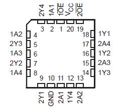 Specifications
Supply voltage range, VCC . . . . . . . . . . . . . . . . . . . . . . . . . . . . . . . . . . . . . . . . . . . . . . . . . . .. 0.5 V to 4.6 V
Input voltage range, VI (see Note 1) . . . . . . . . . . . . . . . . . . . . . . . . . . . . . . . . . . . . . . . . . . . . . 0.5 V to 7 V
Voltage range applied to any output in the high state or power-off state, VO (see Note 1) . . .. 0.5 V to 7 V
Current into any output in the low state, IO: SN54LVTZ244 . . . . . . . . . . . . . . . . . . . . . . . . . . . . . . . . . 96 mA
SN74LVTZ244 . . . . . . . . . . . . . . . . . . . . . . . . . .. . . . . . . 128 mA
Current into any output in the high state, IO (see Note 2): SN54LVTZ244 . . . . . . . . . . . . . . . . . . . . . . 48 mA
SN74LVTZ244 . . . . . . . . . . . . . . . . . . . . . . 64 mA
Input clamp current, IIK (VI < 0) . . . . . . . . . . . . . . . . . . . . . . . . . . . . . . . . . . . . . . . . . . . . . . . . . . . . ..50 mA
Output clamp current, IOK (VO < 0) . . . . . . . . . . . . . . . . . . . . . . . . . . . . . . . . . . . . . . . . . . . . . . . . . . . 50 mA
Maximum power dissipation at TA = 55°C (in still air) (see Note 3): DB package . . . . . . . . . . . . . . . . . . 0.6 W
DW package . . . . . . . . . . . . . . . . . 1.6 W
PW package . . . . . . . . . . . . . .. . . . 0.7 W
Operating free-air temperature range, TA: SN54LVTZ244 . . . . . . . . . . . . . . . . . . . . . . . . . . 55°C to 125°C
SN74LVTZ244 . . . . . . . . . . . . . . . . . . . . . . . . . .. . 40°C to 85°C
Storage temperature range, Tstg . . . . . . . . . . . . . . . . . . . . . . . . . . . . . . . . . . . . . . . . . . . . . 65°C to 150°C
† Stresses beyond those listed under "absolute maximum ratings" may cause permanent damage to the device. These are stress ratings only, and functional operation of the device at these or any other conditions beyond those indicated under "recommended operating conditions" is not implied. Exposure to absolute-maximum-rated conditions for extended periods may affect device reliability.
NOTES: 1. The input and output negative-voltage ratings may be exceeded if the input and output clamp-current ratings are observed.
2. This current flows only when the output is in the high state and VO > VCC.
3. The maximum package power dissipation is calculated using a junction temperature of 150°C and a board trace length of 750 mils. For more information, refer to the Package Thermal Considerations application note in the 1994 ABT Advanced BiCMOS Technology Data Book, literature number SCBD002B.
DescriptionThese octal buffers/drivers of SN54LVTZ244 are designed specifically for low-voltage (3.3-V) VCC operation with the capability to provide a TTL interface to a 5-V system environment.
SN54LVTZ244 is organized as two 4-bit line drivers with separate output-enable (OE) inputs. When OE is low, the device passes data from the A inputs to the Y outputs. When OE is high, the outputs are in the high-impedance state.
Active bus-hold circuitry of SN54LVTZ244 is provided to hold unused or floating data inputs at a valid logic level.
The SN74LVTZ244 is available in TI's shrink small-outline package (DB), which provides the same I/O pin count and functionality of standard small-outline packages in less than half the printed-circuit-board area.
The SN54LVTZ244 is characterized for operation over the full military temperature range of 55°C to 125°C. The SN74LVTZ244 is characterized for operation from 40°C to 85°C.

 SN54LVTZ244 Data Sheet


