Pinout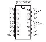 Specifications
| |
SN55109A
SN55110A |
SN75109A
SN75110A |
SN75112 |
UNIT |
| Supply voltage, VCC+ (see Note 1) |
7 |
7 |
7 |
V |
| Supply voltage, VCC |
7 |
7 |
7 |
V |
| Input voltage, VI |
5.5 |
5.5 |
5.5 |
V |
| Output voltage range, VO |
5 to 12 |
5 to 12 |
5 to 12 |
V |
| Continuous total power dissipation (see Note 2) |
See Dissipation Rating Table |
| Operating free-air temperature range, TA |
55 to 125 |
0 to 70 |
0 to 70 |
|
| Storage temperature range, Tstg |
65 to 150 |
65 to 150 |
65 to 150 |
|
| Case temperature for 60 seconds: FK package |
260 |
|
|
|
| Lead temperature 1,6 mm (1/16 inch) from case for 60 seconds |
J or W package |
300 |
|
|
|
| Lead temperature 1,6 mm (1/16 inch) from case for 10 seconds |
D or N package |
|
260 |
260 |
|
Description The SN55109A, SN55110A, SN75109A, SN75110A, and SN75112 dual line drivers have improved output current regulation with supply voltage and temperature variations. In addition, the higher current of the SN75112 (27 mA) allows data to be transmitted over longer lines. These drivers offer optimum performance when used
with the SN55107A, SN55108A, SN75107A, and SN75108A line receivers. SN55109A, SN55110A, SN75109A, SN75110A, and SN75112 feature independent channels with common voltage supply and ground terminals.
The significant difference between the three drivers is in the output current specification. The driver circuits of SN55109A, SN55110A, SN75109A, SN75110A, and SN75112 feature a constant output current that is switched to either of two output terminals by the appropriate logic levels at the input terminals. The output current can be switched off (inhibited) by low logic levels on the enable inputs. The output current is nominally 6 mA for the '109A, 12 mA for the '110A, and 27 mA for the SN75112.
The enable/inhibit feature is provided so the circuits of SN55109A, SN55110A, SN75109A, SN75110A, and SN75112 can be used in party-line or data-bus applications. A strobe
or inhibitor (enable D), common to both drivers, is included for increased driver-logic versatility. The output current in the inhibited mode, IO(off), is specified so that minimum line loading is induced when the driver is used in a party-line system with other drivers. The output impedance of the driver in the inhibited mode is very high.
The output impedance of a transistor is biased to cutoff.

 SN55109A Data Sheet