SN55LBC173

Features: · Meets EIA Standards RS-422-A, RS-423-A, RS-485, and CCITT V.11· Designed to Operate With Pulse Durations as Short as 20 ns· Designed for Multipoint Bus Transmission on Long Bus Lines in Noisy Environments· Input Sensitivity . . . ±200 mV· Low-Power Consumption . . . 20 mA Max· Op...

product image

SN55LBC173 Picture
SeekIC No. : 004497275 Detail

SN55LBC173: Features: · Meets EIA Standards RS-422-A, RS-423-A, RS-485, and CCITT V.11· Designed to Operate With Pulse Durations as Short as 20 ns· Designed for Multipoint Bus Transmission on Long Bus Lines ...

floor Price/Ceiling Price

Part Number:
SN55LBC173
Supply Ability:
5000

Price Break

  • Qty
  • 1~5000
  • Unit Price
  • Negotiable
  • Processing time
  • 15 Days
Total Cost: $ 0.00

SeekIC Buyer Protection PLUS - newly updated for 2013!

  • Escrow Protection.
  • Guaranteed refunds.
  • Secure payments.
  • Learn more >>

Month Sales

268 Transactions

Rating

evaluate  (4.8 stars)

Upload time: 2025/12/24

Payment Methods

All payment methods are secure and covered by SeekIC Buyer Protection PLUS.

Notice: When you place an order, your payment is made to SeekIC and not to your seller. SeekIC only pays the seller after confirming you have received your order. We will also never share your payment details with your seller.
Product Details

Description


Features:

· Meets EIA Standards RS-422-A, RS-423-A,
  RS-485, and CCITT V.11
· Designed to Operate With Pulse Durations
  as Short as 20 ns
· Designed for Multipoint Bus Transmission
  on Long Bus Lines in Noisy Environments
· Input Sensitivity . . . ±200 mV
· Low-Power Consumption . . . 20 mA Max
· Open-Circuit Fail-Safe Design
· Pin Compatible With SN75173 and
  AM26LS32


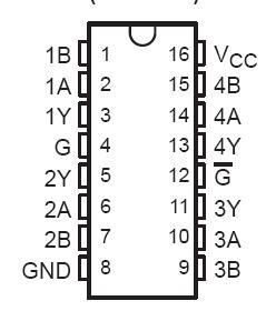
Pinout

  Connection Diagram


Specifications

Supply voltage range, VCC (see Note 1) . . . . . . . . . . . . . . . . . . . . . . . . . . . . . . . . . . . . . . . . . . . .0.3 V to 7 V
Input voltage, VI (A or B inputs) . . . . . . . . . . . . . . . . . . . . . . . . . . . . . . . . . . . . . . . . . . . . . . . . . . . . . . . ±25 V
Differential input voltage, VID (see Note 2) . . . . . . . . . . . . . . . . . . . . . . . . . . . . . . . . . . . . . . . . . . . . . . . ±25 V
Data and control voltage range . . . . . . . . . . . . . . . . . . . . . . . . . . . . . . . . . . . . . . . . . . . . . . . . . . 0.3 V to 7 V
Continuous total dissipation . . . . . . . . . . . . . . . . . . . . . . . . . . . . . . . . . . . . . . . . .See Dissipation Rating Table
Operating free-air temperature range, TA . . . . . . . . . . . . . . . . . . . . . . . . . . . . . . . . . . . . . . . . 55°C to 125°C
Storage temperature range, Tstg . . . . . . . . . . . . . . . . . . . . . . . . . . . . . . . . . . . . . . . . . . . . . . .65°C to 150°C
Lead temperature 1,6 mm (1/16 inch) from case for 10 seconds . . . . . . . . . . . . . . . . . . . . . . . . . . . . . . .260°C
† Stresses beyond those listed under "absolute maximum ratings" may cause permanent damage to the device. These are stress ratings only, and
functional operation of the device at these or any other conditions beyond those indicated under "recommended operating conditions" is not
implied. Exposure to absolute-maximum-rated conditions for extended periods may affect device reliability.
NOTES: 1. All voltage values are with respect to GND.
2. Differential input voltage is measured at the noninverting input with respect to the corresponding inverting input.


Description

The SN55LBC173 is a monolithic quadruple differential line receiver with 3-state outputs and is designed to meet the requirements of the EIA standards RS-422-A, RS-423-A, RS-485, and CCITT V.11. SN55LBC173 is optimized for balanced multipoint bus transmission at data rates up to and exceeding 10 million bits per second. The four receivers share two ORed enable inputs, one active when high, the other active when low. Each receiver features high input impedance, input hysteresis for increased noise immunity, and input sensitivity of ±200 mV over a common-mode input voltage range of 12 V to 7 V. Fail-safe design ensures that if the inputs are open circuited, the output is always high. The SN55LBC173 is designed using the Texas Instruments proprietary LinBiCMOSEtechnology that provides low power consumption, high switching speeds, and robustness.

This device offers optimum performance when used with the SN55LBC172M quadruple line driver. The SN55LBC173 is available in the 16-pin CDIP (J), the 16-pin CPAK (W), or the 20-pin LCCC (FK) packages. The SN55LBC173 is characterized over the military temperature range of 55°C to 125°C.


Customers Who Bought This Item Also Bought

Margin,quality,low-cost products with low minimum orders. Secure your online payments with SeekIC Buyer Protection.
Potentiometers, Variable Resistors
Discrete Semiconductor Products
Sensors, Transducers
Industrial Controls, Meters
Programmers, Development Systems
View more