Features: Meet or Exceed the Requirements of ANSI TIA/EIA-644 Standard
Operate With a Single 3.3-V Supply
Designed for Signaling Rate of up to 400 Mbps
Differential Input Thresholds ±100 mV Max
Typical Propagation Delay Time of 2.1 ns
Power Dissipation 60 mW Typical Per Receiver at 200 MHz
Bus-Terminal ESD Protection Exceeds 8 kV
Low-Voltage TTL (LVTTL) Logic Output Levels
Pin Compatible With AM26LS32, MC3486,and A9637
Open-Circuit Fail-SafeApplicationAudio www.ti.com/audio
Automotive www.ti.com/automotive
Broadband www.ti.com/broadband
Digital Control www.ti.com/digitalcontrol
Military www.ti.com/military
Optical Networking www.ti.com/opticalnetwork
Security www.ti.com/security
Telephony www.ti.com/telephony
Video & Imaging www.ti.com/video
Wireless www.ti.com/wirelessPinout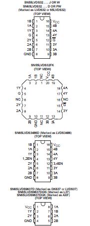 SpecificationsSupply voltage range, VCC (see Note 1) . . . . . . . . . . . . . . . . . . . . −0.5 V to 4 V
Input voltage range, VI (enables and output) . . . . . . . . . −0.5 V to VCC + 0.5 V
Input voltage range, VI (A or B) . . . . . . . .. . . . . . . . .. . . . . . . . . . . −0.5 V to 4 V
Continuous total power dissipation . . . . . . . . . . . . See Dissipation Rating Table
Lead temperature 1,6 mm (1/16 inch) from case for 10 seconds . . . . . . . . 260
Storage temperature range, Tstg .. . . . . . . . . . . . . . . . . . . . . . . . −65 to 150
† Stresses beyond those listed under "absolute maximum ratings" may cause permanent damage to the device. These are stress ratings only, and functional operation of the device at these or any other conditions beyond those indicated under "recommended operating conditions" is not implied. Exposure to absolute-maximum-rated conditions for extended periods may affect device reliability.
NOTE 1: All voltages, except differential I/O bus voltages, are with respect to the network ground terminal.DescriptionThe SN55LVDS32, SN65LVDS32,SN65LVDS3486, and SN65LVDS9637 are differential line receivers that implement the electrical characteristics of low-voltage differential signaling (LVDS). This signaling technique lowers the output voltage levels of 5-V differential standard levels (such as EIA/TIA-422B) to reduce the power, increase the switching speeds, and allow operation with a 3.3-V supply rail. Any of the four differential receivers SN55LVDS32, SN65LVDS32,SN65LVDS3486, and SN65LVDS9637 provides a valid logical output state with a ±100-mV differential input voltage within the input common-mode voltage range. The input common-mode voltage range allows 1 V of ground potential difference between two LVDS nodes.
The intended application of SN55LVDS32, SN65LVDS32,SN65LVDS3486, and SN65LVDS9637 and signaling technique is both point-to-point and multidrop (one driver and multiple receivers) data transmission over controlled impedance media of approximately 100 . The transmission media SN55LVDS32, SN65LVDS32,SN65LVDS3486, and SN65LVDS9637 may be printed-circuit board traces, backplanes,or cables. The ultimate rate and distance of data transfer depends on the attenuation characteristics of the media and the noise coupling to the environment.

 SN55LVDS32 Data Sheet