SN64BCT541A

Features: • BiCMOS Design Significantly Reduces Standby Current• 3-State True Outputs Drive Bus Lines or Buffer Memory-Address Registers• High-Impedance State During Power Up and Power Down• P-N-P Inputs Reduce DC Loading• Data Flow-Through Pinout (All Inputs on Oppos...

product image

SN64BCT541A Picture
SeekIC No. : 004497312 Detail

SN64BCT541A: Features: • BiCMOS Design Significantly Reduces Standby Current• 3-State True Outputs Drive Bus Lines or Buffer Memory-Address Registers• High-Impedance State During Power Up and P...

floor Price/Ceiling Price

Part Number:
SN64BCT541A
Supply Ability:
5000

Price Break

  • Qty
  • 1~5000
  • Unit Price
  • Negotiable
  • Processing time
  • 15 Days
Total Cost: $ 0.00

SeekIC Buyer Protection PLUS - newly updated for 2013!

  • Escrow Protection.
  • Guaranteed refunds.
  • Secure payments.
  • Learn more >>

Month Sales

268 Transactions

Rating

evaluate  (4.8 stars)

Upload time: 2025/12/24

Payment Methods

All payment methods are secure and covered by SeekIC Buyer Protection PLUS.

Notice: When you place an order, your payment is made to SeekIC and not to your seller. SeekIC only pays the seller after confirming you have received your order. We will also never share your payment details with your seller.
Product Details

Description


Features:

• BiCMOS Design Significantly Reduces Standby Current
• 3-State True Outputs Drive Bus Lines or Buffer Memory-Address Registers
• High-Impedance State During Power Up and Power Down
• P-N-P Inputs Reduce DC Loading
• Data Flow-Through Pinout (All Inputs on Opposite Side From Outputs)
• ESD Protection Exceeds 2000 V Per MIL-STD-883C, Method 3015
• Package Options Include Plastic Small-Outline (DW) Packages and Standard Plastic (N) 300-mil DIPs


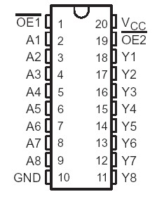
Pinout

  Connection Diagram


Specifications

Supply voltage range, VCC . . . . . . . . . . . . . . . . . . . . . . . . . . . . . . . . . . . . . . . . . . . . . . . . . .0.5 V to 7 V
Input voltage range, VI (see Note 1) . . . . . . . . . . . . . . . . . . . . . . . . . . . . . . .  . . . . . . . . . . 0.5 V to 7 V
Voltage range applied to any output in the disabled or power-off state, VO . . . . . . . .  . .0.5 V to 5.5 V
Voltage range applied to any output in the high state, VO . . . . . . . . . . . . . . . . . . . . . . . . .0.5 V to VCC
Current into any output in the low state  . . . . . . . . . . . . . . . . . . . . . . . . . . . .  . . . . . . . . . . . . . . .128 mA
Operating free-air temperature range, TA . . . . . . . . . . . . . . . . . . . . . . . . . . . . .. . . . . . . . .40°C to 85°C
Storage temperature range . . . . . . . . . . . . . . . . . . . . . . . . . . . . . . . . . . . . . .. . . . . . . . . .65°C to 150°C


Description

The SN64BCT541A octal buffer and line driver is ideal for driving bus lines or buffering memory-address registers. The device features inputs and outputs on opposite sides of the package to facilitate printed-circuit-board layout.

The 3-state control gate is a 2-input AND gate with active-low inputs of SN64BCT541A so that if either output-enable (OE1 or OE2) input is high, all eight outputs are in the high-impedance state. The outputs of SN64BCT541A are in a high-impedance state during power up and power down while the supply voltage is less than approximately 3 V.

The SN64BCT541A is characterized for operation from 40°C to 85°C and from 0°C to 70°C.


Customers Who Bought This Item Also Bought

Margin,quality,low-cost products with low minimum orders. Secure your online payments with SeekIC Buyer Protection.
RF and RFID
Industrial Controls, Meters
Undefined Category
Fans, Thermal Management
Static Control, ESD, Clean Room Products
View more